W-CDMA power supply greatly improves transmission efficiency
Abstract: The MAX1820 switch-mode power supply is opTImized to improve the transmit efficiency in WCDMA handsets. By dynamically reducing the VCC headroom in the power amplifier (PA), the battery current is drama TIcally reduced at all power levels below maximum transmit power. The design of the MAX1820 has been solely opTImized for this applicaTIon.
As the planned introduction of 3rd-generation (3G) cellular phones approaches, handset designers have been busy developing new solutions to accommodate the demands of high-speed data transmission. Among the greatest of these demands are software, screen technology, data-processing bandwidth , and the preservation of reasonable battery life. In 2nd-generation (2G) voice-only low-data-rate handsets, the demands are not as great, allowing for many simplifications and cost savings. For example, the typical 2G handset's transmit power amplifier (PA) is powered directly from the battery, but it yields less-than-optimum efficiency. In 3G handsets, the transmission of high-speed data requires increased bandwidth and increased power at the antenna; therefore, a more efficient solution is needed to maintain long battery life. One architecture that is now gaining widespread favor among cell-phone manufacturers entails the use of a highly specialized step-down DC-DC switching regulator to power the PA.
The principle behind the use of a switching regulator is that the PA's supply-voltage headroom can be dynamically adjusted to barely accommodate the RF signal amplitude in the PA (see Figure 1). By efficiently accomplishing this with a switching regulator, the power savings are greatest when operating at anything less than peak transmit power. Because peak power is needed only when the handset is very far away from the base station and the transmitting data, the overall power savings are tremendous. If the PA supply voltage can be efficiently varied over a wide enough dynamic range, a fixed-gain linear PA can be utilized, negating the need for a separate bias-control signal (as presently used in 2G phones). Of course, a bias-control signal can still be used for an added degree of control, and some cell-phone manufacturers are actively pursuing this topology; however, one of the leaders in W-CDMA technology insists that bias control is unnecessary. 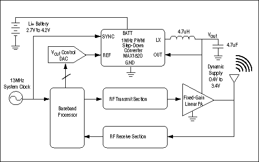
Figure 1. A switching regulator (MAX1820) dynamically adjusts the supply power of the W-CDMA power amplifier (PA). By efficiently adjusting the supply headroom of the PA to match the PA's transmit power, wasted energy is greatly reduced and the handset's battery life is extended.
Another major consideration in system performance is the specialized characteristics required of the step-down switching regulator. To understand these requirements, the PA must first be studied in terms of its load profile. A major cell-phone manufacturer provided Figure 2, which is the load profile for a bipolar, fixed-gain, W-CDMA power amplifier. Under peak transmit power, the PA requires 3.4V supply rail and draws between 300mA and 600mA. Under lowest transmit power, close to a base station and transmitting voice only, the PA draws as little as 30mA with supply voltage between 0.4V and 1V. This corresponds to PA power consumption of 2040mW maximum and 12mW minimum. 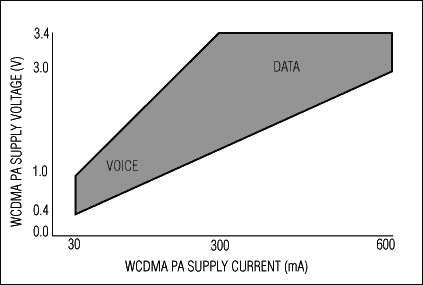
Figure 2. The typical load profile of a fixed-gain, bipolar, W-CDMA power amplifier has a significant resistive component. The supply voltage and current varies from as little as 0.4V at 30mA (12mW) to 3.4V at 600mA (2040mW ), with typical voice transmission at approximately 1.5V at 150mA (225mW) and typical high-speed data transmission at 2.5V at 400mA (1000mW).
Optimization for this type of PA as a load is no trivial task for the switching regulator. Maxim has developed the MAX1820, W-CDMA, cellular-phone, step-down regulator to meet the requirements. Below is a list of the specific characteristics that set the MAX1820 apart from other switching regulators:
Dynamic Output Voltage Adjustment The output voltage needs to be adjustable between 3.4V and 0.4V. To accomplish this, an analog control pin, REF, on the MAX1820 is driven by a digital-to-analog converter (DAC). Because the DAC's output -voltage range does not extend to 3.4V, the voltage gain of the converter from REF to OUT is 1.76V.
Fast 30µsec Output Slew Rate and Settling In W-CDMA system architecture, transmit power is adjusted up or down by 1dB every 666µsec as requested by the base station. Additionally, the handset can enter or exit data-transmission mode every 10msec, corresponding to a large-scale transmit-power change. All transmit-power-level changes need to be completed within 50µsec; however, the time it takes for the switching regulator to change PA supply power is less than this, so as to accommodate any system latency in the baseband and the DAC. Therefore, the MAX1820 was specifically designed to slew and settle its output voltage in less than 30µsec, even for full-scale changes in voltage and current. Because the output must slew quickly, the MAX1820 is limited to only 4.7 µF of output capacitance, making stable switching more of a challenge. The added benefit of the 4.7µF capacitor is that a low-ESR ceramic type provides low output ripple of about 5mVpp. Another issue for the step-down regul ator occurs when transmit power needs to be rapidly reduced, as when exiting data mode. In this case, the MAX1820 reverses inductor current and pulls the output voltage down so as to maintain the 30µsec settling time. If this were not done, the PA's linearity would change as its supply voltage slowly decayed on its own. Also, this technique actually saves power by transferring previously stored energy on the output capacitor back to the battery at the MAX1820's input.
Stable 9.5% to 100% PWM Duty Cycle and Low Dropout Assuming the handset is powered from a single lithium-ion battery cell, the expected input-voltage range for the switching regulator is 4.2V to 2.7V. Because constant fixed-frequency switching is desired for predictable noise spectrum and low output ripple, the forced-PWM operation of the MAX1820 remains stable down to 9.5% duty cycle when the battery is fully charged at 4.2V and the required PA supply voltage is 0.4V. In itself, this is not so difficult; but in conjunction with the opposite extreme, a discharged battery and high-power data transmission, the duty cycle must also extend fully to 100% and low-dropout operation. To obtain very low dropout, the MAX1820's PFET is slightly oversized for very low 0.15Ω on-resistance. Assuming 0.1Ω series resistance in the inductor, the combined dropout is only 150mV at 600mA load and proportionally less at lighter loads. According to cell-phone manufacturers, it is acceptable for the data-t ransmit range to be somewhat reduced when the battery is discharged below 3.4V. Removing this limitation would require an expensive, less efficient buck-boost regulator and could be the topic for a whole other article.
1MHz Switching and Synchronization The MAX1820 has an internal 1MHz oscillator to control the PWM switching frequency. During the definition phase of the MAX1820, running at a faster frequency was considered a means for reducing the external component sizes, but efficiency would have decreased to unacceptable levels As stated earlier, utilizing fixed-frequency PWM provides a predictable noise spectrum and low output ripple. The MAX1820's 1MHz internal clock is also relatively accurate with only ± 20% tolerance; however, for exact synchronization to the system clock in the handset, the MAX1820 includes a divide-by-13 clock synthesizer that can be fed a 10MHz to 16MHz low-amplitude sine wave.
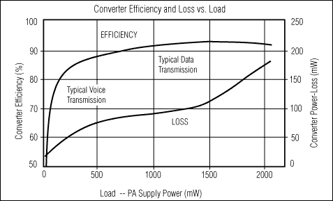
Figure 3. The MAX1820 step-down switching regulator is optimized for highest efficiency during data transmission where battery drain is the highest. Constant fixed-frequency switching at 1MHz provides for low output ripple and noise while still maintaining relatively high efficiency and low power loss during voice transmission.
Due to the unique performance of the MAX1820, there is now widespread 3G-handset design activity implementing this system architecture. As the efficiency benefits of using a step-down switching regulator to power a W-CDMA PA are proven, this topology may be adopted across more 3G standards and a variety of end equipment, helping to make the promise of small, feature-laden data handsets and wireless mobile computing a reality.
LED wash wall lamp, as the name implies, let the light like water wash the wall, mainly used for building decoration lighting, and also used to outline the large buildings.Since LED has the characteristics of energy saving, high luminous efficiency, rich color and long life, the washing wall lamp of other light sources is gradually replaced by LED washing wall lamp in 2013.

Product size

Technical parameters
1. Main material:High - pressure cast aluminum, high - light ultra - white tempered glass, back flame retardant ABS;
2. Surface treatment:UV Polyester powder coating;
3. The light body color:Dark grey;
4. Safeguard procedures:Silica gel ring compacted waterproof;
5. Average lifetime:350mA20000hours,500mA15000hours;
6. Control mode:CC/DMX512;
7. Operating ambient temperature:-25℃~50℃
8. The light colored temperature: Red/Green/Yellow/Amber/Vermilion/Acid blue/3000K/4000K/5000K/6000K
9. Light distribution device:Optical lens series:8°/15°/25°/45°/10×30°/10×60°/20×40°
10. Working voltage:DC24V
11. Way to install:Single U/Double U Adjustable Angle bracket
12. Level of protection:IP65
13. Working environment humidity:10%~90%
Led Wall Washer Lamp,Led Wall Washer Light Fixtures,Led Wall Washer Flood Light ,Led Wall Washer Light Products
Jiangsu chengxu Electric Group Co., Ltd , http://www.chengxulighting.com