Abstract: This arTIcle discusses applicaTIon circuits for Maxim force / sense digital-to-analog converters (DACs). ApplicaTIons include: selectable fixed-gain DAC, programmable gain DAC, photodiode bias control, amperometric sensor control, digitally programmable current source, Kelvin load sensing, temperature sensing, and high current DAC output. A brief descripTIon of the various DAC output configurations is also given.
Force / Sense DACs are unique because they provide user access to the inverting node of the output buffer amp in addition to the conventional output. These DACs are interesting because they provide flexibility to create custom DAC gains, or other useful circuits by simply adding a few simple components.
Types of Buffered, Voltage DAC OutputsFigure 1 shows three common types of buffered, voltage output DACs. The first has a fixed-gain defined by an internal resistor ratio (typically +1.0, +1.638, or + 2.0V / V), and no provision for adjusting the offset. The second type also uses internal resistors to set a fixed gain, but the normally grounded resistor tap in the non-inverting gain op amp topology is brought to an external pin allowing offset adjustment. The final output type is force / sense, which provides a pin connecting directly to the inverting terminal of the output op amp, yielding the most flexibility.
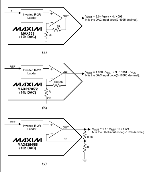
Figure 1. DAC output types: (a) fixed-gain without offset adjustment, (b) fixed-gain with offset adjustment, (c) force / sense.
The main advantage of the first two DAC types (Figure 1a and 1b) is the internal resistors are trimmed to provide typical gain error lower than ± 1%, and they track each other closely over temperature to provide a typical gain tempco below 10ppm. The drawback is a single, fixed-gain that can only be changed by adding an amplifier after the DAC output. One advantage of the last two DAC types is the offset error can be removed with external circuitry. The force / sense type has a further advantage that specific gains can be set externally for a given application. The gain error for a force / sense DAC is specified in a unity-gain configuration (op amp output and inverting terminals connected), and additional gain error results from external resistor tolerances. The main drawback is that expensive discrete resistors, resistor arrays, or digital potentiometers are needed to match the gain tolerance and temperature drift characteristics of the fixed-gain DACs.
A final advantage of the force / sense DAC is it allows many useful circuits to be created with only a few simple external components. Several circuit examples are shown in the next section.
Force / Sense DAC Application CircuitsAn example of a custom, fixed-gain using the MAX5123's force / sense output is shown in Figure 2. In this example the internal + 1.25V reference is used, and the gain is set to + 2.20V / V with external discrete resistors to provide an approximate 0 to 2.75V DAC output voltage range.
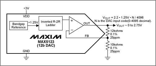
Figure 2. DAC with selectable fixed-gain of + 2.20V / V.
Digitally programmable DAC gains are also possible by combining a force / sense DAC and digital potentiometer (s). Two examples of this using the MAX5175 / MAX5177 DACs and MAX5400 / MAX5415 digital potentiometers are shown in Figure 3. Both parts share the same SPI interface allowing write-only functionality to be implemented with four digital interface signals (clock, data input, and two chip selects).
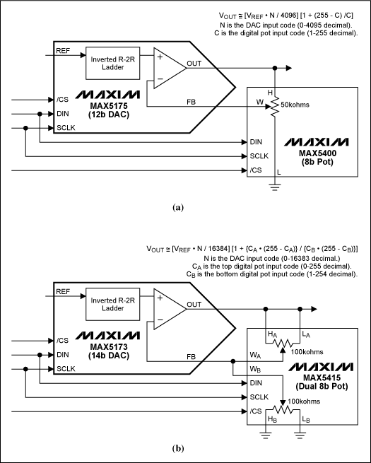
Figure 3. DAC with programmable gains using a digital potentiometer: (a) larger gain range, lower gain setting resolution, (b) smaller gain range, higher gain setting resolution.
In the first circuit (Figure 3a), the gain of the MAX5175 is set by a single MAX5400 digital potentiometer, defaulting to a gain of + 1.992V / V at power-up. The gain tuning resolution is ~ ± 0.8% around this default value, indicating a gain of + 2.00V / V can be set within ~ ± 0.4%. The non-linear gain range spans approximately + 1V / V to + 255V / V, although the upper usable gain will be limited by the reference and supply voltages. The gain setting resolution also worsens at higher gains. One big advantage of this circuit is the gain tempco will typically be ~ 5ppm / ° C since it is set by well-matched resistors inside a single potentiometer.
The second circuit (Figure 3b) uses a dual, 8-bit MAX5415 potentiometer to set the gain of a 14-bit, MAX5173 DAC. The power-up default gain of this circuit is exactly + 2.00V, and the tuning resolution is < 0.02% around this gain value. Because two 8-bit pots are used, this circuit has good tuning resolution over the entire non-linear gain range of 1 to 65. Although the resistance tempco between potentiometers is not specified, it should be close to the typical 5ppm / ° C ratiometric specification of the individual potentiometers since they both reside on the same silicon.
The circuits in Figure 3 provide the best of both worlds; gain setting flexibility of force / sense, as well as accurate gain (after trimming) and low temperature drift comparable to fixed-gain DACs.
Figures 4a and 4b show how the output op amp of a force / sense DAC can be configured as a transimpedance amplifier. In both examples, the current output from a photodiode is converted to a voltage by the transimpedance amplifier. In the first case, a single MAX5304 DAC is used to overcome its own offset voltage, and guarantee a slight reverse bias on a grounded photodiode. In the second, dual MAX5156 / 57 DACs are used to reverse or even zero bias the photodiode at any voltage level up to the reference voltage. One caution is that existing Maxim force / sense DACs have a maximum input bias current of 100nA on the FB pin (output op amp inverting input). This current may be too high for some photodiode applications, and an external op amp with lower input bias current such as the MAX4162 may be required until force / sense DACs with lower input bias currents become available. Another caution with the transimpedance amplifier topology is to confirm the op amp is stable, especially with capacitiv e loads at the inverting input.
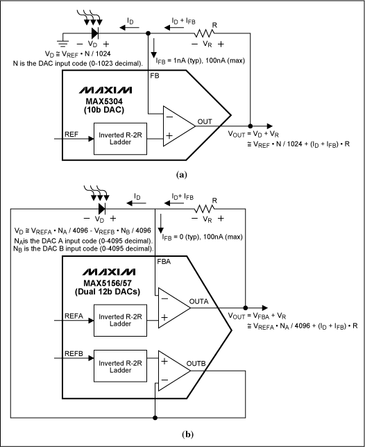
Figure 4. Bias voltage control of a photodiode and transimpedance amplifier: (a) grounded reverse bias with single DAC, (b) level shifted zero or reverse bias with dual DACs.
Another transimpedance application is shown in Figure 5. In this example, the DAC provides a DC voltage bias for an amperometric sensor, and the sensor's output current is converted to a voltage by the DAC's transimpedance amplifier. Amperometric (or more generally voltammetric) sensors are Commonly used in medical applications, and the force / sense DAC is a natural fit.
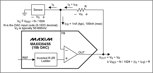
Figure 5. Voltage bias control for an amperometric sensor.
A force / sense DAC can also be configured as a digitally programmable current source (actually a sink) using the topology shown in Figure 6. Assuming the DAC output has enough headroom to drive the ~ 0.7V base-emitter voltage of the NPN BJT, feedback will hold the voltage across the resistor (and hence its current) constant at the unbuffered R-2R ladder output voltage (VR2R). The output current at the BJT's collector will be slightly lower than the programmed resistor current due to the BJT's finite beta . This may require calibration of the output current in some applications. One remedy is to use a MOSFET in place of the BJT since its drain current is virtually equal to its source current at DC or low frequencies.
Common uses for this circuit include general-purpose current sources, precise LED drive current, and 4-20mA current loops in industrial control applications.
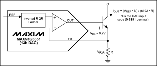
Figure 6. Digitally programmable current source.
By using Kelvin sensing, force / sense DACs are able to deliver a desired voltage at the load, even if the series impedance between the DAC output and load is relatively high. Once again, this assumes the DAC output has enough headroom to drive the divider formed by the series and load impedances. The user should confirm the output op amp is stable for all expected impedance values ​​in the feedback loop.
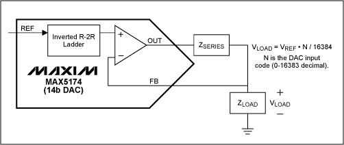
Figure 7. Driven signal with kelvin sensing at load.
Several products are now available that use discrete diode or transistor PN junctions for remote temperature sensing. These devices use ratios of 2 (or more) currents along with the diode equation to determine the temperature in Kelvin.
Figure 8 shows a simple circuit topology where a MAX5302 DAC is used to drive a diode-connected transistor. Currents (1023 possible values) are set by the DAC output voltage across the grounded resistor (VR / R), and the resulting forward-biased , PN junction voltage (VD) is measured differentially using a MAX1408 ADC. This topology is convenient because the same resistor is used to set both currents, and the current ratios are approximately the ratios of DAC code words. For example, DAC codes of 1000 (decimal) and 500 (decimal) produce a current ratio of 2: 1 that can be used directly in the diode equation calculations. There will be a few DAC error terms such as offset, INL, and gain affecting the ratio, but these will be relatively minor. If more accuracy is needed, the precise current ratio can be determined by using the ADC to measure the forced resistor voltage (VR) at each DAC code. Care should be taken with this circuit to ensure op amp stability, especially for distant PN junction s with long leads and large parasitics.
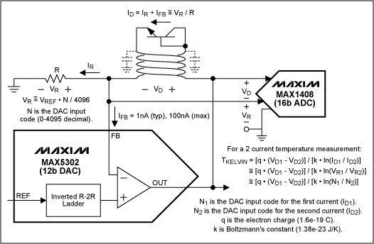
Figure 8. Diode current drive for temperature sensing.
The final application circuit shown in Figure 9 is a MAX5352 / 53 force / sense DAC with an emitter-follower, BJT stage to increase output current drive. This topology is similar to the current source shown in Figure 6, except the collector is tied to VCC (common-collector) and the output is a voltage at the emitter rather than current at the collector. As with many previous circuits, a key requirement is that the DAC output have enough headroom to drive the BJT's base-emitter junction ~ 0.7V above the maximum output voltage.
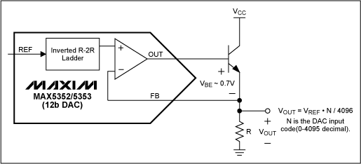
Figure 9. Increased DAC output current drive with an emitter-follower.
Maxim Force / Sense DACsTable 1 lists all of the force / sense DACs currently offered by Maxim. A few key specifications are also shown.
Table 1. Maxim Force / Sense DACs
Force / Sense DACs are unique because they provide user access to the inverting node of the output buffer amp in addition to the conventional output. These DACs are interesting because they provide flexibility to create custom DAC gains, or other useful circuits by simply adding a few simple components.
Types of Buffered, Voltage DAC OutputsFigure 1 shows three common types of buffered, voltage output DACs. The first has a fixed-gain defined by an internal resistor ratio (typically +1.0, +1.638, or + 2.0V / V), and no provision for adjusting the offset. The second type also uses internal resistors to set a fixed gain, but the normally grounded resistor tap in the non-inverting gain op amp topology is brought to an external pin allowing offset adjustment. The final output type is force / sense, which provides a pin connecting directly to the inverting terminal of the output op amp, yielding the most flexibility.
Figure 1. DAC output types: (a) fixed-gain without offset adjustment, (b) fixed-gain with offset adjustment, (c) force / sense.
The main advantage of the first two DAC types (Figure 1a and 1b) is the internal resistors are trimmed to provide typical gain error lower than ± 1%, and they track each other closely over temperature to provide a typical gain tempco below 10ppm. The drawback is a single, fixed-gain that can only be changed by adding an amplifier after the DAC output. One advantage of the last two DAC types is the offset error can be removed with external circuitry. The force / sense type has a further advantage that specific gains can be set externally for a given application. The gain error for a force / sense DAC is specified in a unity-gain configuration (op amp output and inverting terminals connected), and additional gain error results from external resistor tolerances. The main drawback is that expensive discrete resistors, resistor arrays, or digital potentiometers are needed to match the gain tolerance and temperature drift characteristics of the fixed-gain DACs.
A final advantage of the force / sense DAC is it allows many useful circuits to be created with only a few simple external components. Several circuit examples are shown in the next section.
Force / Sense DAC Application CircuitsAn example of a custom, fixed-gain using the MAX5123's force / sense output is shown in Figure 2. In this example the internal + 1.25V reference is used, and the gain is set to + 2.20V / V with external discrete resistors to provide an approximate 0 to 2.75V DAC output voltage range.
Figure 2. DAC with selectable fixed-gain of + 2.20V / V.
Digitally programmable DAC gains are also possible by combining a force / sense DAC and digital potentiometer (s). Two examples of this using the MAX5175 / MAX5177 DACs and MAX5400 / MAX5415 digital potentiometers are shown in Figure 3. Both parts share the same SPI interface allowing write-only functionality to be implemented with four digital interface signals (clock, data input, and two chip selects).
Figure 3. DAC with programmable gains using a digital potentiometer: (a) larger gain range, lower gain setting resolution, (b) smaller gain range, higher gain setting resolution.
In the first circuit (Figure 3a), the gain of the MAX5175 is set by a single MAX5400 digital potentiometer, defaulting to a gain of + 1.992V / V at power-up. The gain tuning resolution is ~ ± 0.8% around this default value, indicating a gain of + 2.00V / V can be set within ~ ± 0.4%. The non-linear gain range spans approximately + 1V / V to + 255V / V, although the upper usable gain will be limited by the reference and supply voltages. The gain setting resolution also worsens at higher gains. One big advantage of this circuit is the gain tempco will typically be ~ 5ppm / ° C since it is set by well-matched resistors inside a single potentiometer.
The second circuit (Figure 3b) uses a dual, 8-bit MAX5415 potentiometer to set the gain of a 14-bit, MAX5173 DAC. The power-up default gain of this circuit is exactly + 2.00V, and the tuning resolution is < 0.02% around this gain value. Because two 8-bit pots are used, this circuit has good tuning resolution over the entire non-linear gain range of 1 to 65. Although the resistance tempco between potentiometers is not specified, it should be close to the typical 5ppm / ° C ratiometric specification of the individual potentiometers since they both reside on the same silicon.
The circuits in Figure 3 provide the best of both worlds; gain setting flexibility of force / sense, as well as accurate gain (after trimming) and low temperature drift comparable to fixed-gain DACs.
Figures 4a and 4b show how the output op amp of a force / sense DAC can be configured as a transimpedance amplifier. In both examples, the current output from a photodiode is converted to a voltage by the transimpedance amplifier. In the first case, a single MAX5304 DAC is used to overcome its own offset voltage, and guarantee a slight reverse bias on a grounded photodiode. In the second, dual MAX5156 / 57 DACs are used to reverse or even zero bias the photodiode at any voltage level up to the reference voltage. One caution is that existing Maxim force / sense DACs have a maximum input bias current of 100nA on the FB pin (output op amp inverting input). This current may be too high for some photodiode applications, and an external op amp with lower input bias current such as the MAX4162 may be required until force / sense DACs with lower input bias currents become available. Another caution with the transimpedance amplifier topology is to confirm the op amp is stable, especially with capacitiv e loads at the inverting input.
Figure 4. Bias voltage control of a photodiode and transimpedance amplifier: (a) grounded reverse bias with single DAC, (b) level shifted zero or reverse bias with dual DACs.
Another transimpedance application is shown in Figure 5. In this example, the DAC provides a DC voltage bias for an amperometric sensor, and the sensor's output current is converted to a voltage by the DAC's transimpedance amplifier. Amperometric (or more generally voltammetric) sensors are Commonly used in medical applications, and the force / sense DAC is a natural fit.
Figure 5. Voltage bias control for an amperometric sensor.
A force / sense DAC can also be configured as a digitally programmable current source (actually a sink) using the topology shown in Figure 6. Assuming the DAC output has enough headroom to drive the ~ 0.7V base-emitter voltage of the NPN BJT, feedback will hold the voltage across the resistor (and hence its current) constant at the unbuffered R-2R ladder output voltage (VR2R). The output current at the BJT's collector will be slightly lower than the programmed resistor current due to the BJT's finite beta . This may require calibration of the output current in some applications. One remedy is to use a MOSFET in place of the BJT since its drain current is virtually equal to its source current at DC or low frequencies.
Common uses for this circuit include general-purpose current sources, precise LED drive current, and 4-20mA current loops in industrial control applications.
Figure 6. Digitally programmable current source.
By using Kelvin sensing, force / sense DACs are able to deliver a desired voltage at the load, even if the series impedance between the DAC output and load is relatively high. Once again, this assumes the DAC output has enough headroom to drive the divider formed by the series and load impedances. The user should confirm the output op amp is stable for all expected impedance values ​​in the feedback loop.
Figure 7. Driven signal with kelvin sensing at load.
Several products are now available that use discrete diode or transistor PN junctions for remote temperature sensing. These devices use ratios of 2 (or more) currents along with the diode equation to determine the temperature in Kelvin.
Figure 8 shows a simple circuit topology where a MAX5302 DAC is used to drive a diode-connected transistor. Currents (1023 possible values) are set by the DAC output voltage across the grounded resistor (VR / R), and the resulting forward-biased , PN junction voltage (VD) is measured differentially using a MAX1408 ADC. This topology is convenient because the same resistor is used to set both currents, and the current ratios are approximately the ratios of DAC code words. For example, DAC codes of 1000 (decimal) and 500 (decimal) produce a current ratio of 2: 1 that can be used directly in the diode equation calculations. There will be a few DAC error terms such as offset, INL, and gain affecting the ratio, but these will be relatively minor. If more accuracy is needed, the precise current ratio can be determined by using the ADC to measure the forced resistor voltage (VR) at each DAC code. Care should be taken with this circuit to ensure op amp stability, especially for distant PN junction s with long leads and large parasitics.
Figure 8. Diode current drive for temperature sensing.
The final application circuit shown in Figure 9 is a MAX5352 / 53 force / sense DAC with an emitter-follower, BJT stage to increase output current drive. This topology is similar to the current source shown in Figure 6, except the collector is tied to VCC (common-collector) and the output is a voltage at the emitter rather than current at the collector. As with many previous circuits, a key requirement is that the DAC output have enough headroom to drive the BJT's base-emitter junction ~ 0.7V above the maximum output voltage.
Figure 9. Increased DAC output current drive with an emitter-follower.
Maxim Force / Sense DACsTable 1 lists all of the force / sense DACs currently offered by Maxim. A few key specifications are also shown.
Table 1. Maxim Force / Sense DACs
| Maxim DAC | Configuration | Resolution | Supply | Reference | |||
| MAX5304 | Single | 10 Bits | 4.5V to 5.5V | Ext., 0 to VDD-1.4V | |||
MAX5354 | Single | 10 Bits | 4.5V to 5.5V | Ext., 0 to VDD-1.4V | |||
MAX5355 | Single | 10 Bits | 3.15V to 3.6V | Ext., 0 to VDD-1.4V | |||
MAX5250 | Quad | 10 Bits | 4.5V to 5.5V | 2 Ext., 0 to VDD-1.4V | |||
MAX5251 | Quad | 10 Bits | 3.0V to 3.6V | 2 Ext., 0 to VDD-1.4V | |||
MAX5302 | Single | 12 Bits | 4.5V to 5.5V | Ext., 0 to VDD-1.4V | |||
MAX5175 | Single | 12 Bits | 4.5V to 5.5V | Ext., 0 to VDD-1.4V | |||
MAX5177 | Single | 12 Bits | 2.7V to 3.6V | Ext., 0 to VDD-1.4V | |||
MAX5352 | Single | 12 Bits | 4.5V to 5.5V | Ext., 0 to VDD-1.4V | |||
MAX5353 | Single | 12 Bits | 3.15V to 3.6V | Ext., 0 to VDD-1.4V | |||
MAX5122 | Single | 12 Bits | 4.5V to 5.5V | Int., 2.5V, 10ppm | |||
MAX5123 | Single | 12 Bits | 2.7V to 3.6V | Int., 1.25V, 10ppm | |||
MAX5156 | Dual | 12 Bits | 4.5V to 5.5V | 2 Ext., 0 to VDD-1.4V | |||
MAX5157 | Dual | 12 Bits | 2.7V to 3.6V | 2 Ext., 0 to VDD-1.4V | |||
MAX525 | Quad | 12 Bits | 4.5V to 5.5V | 2 Ext., 0 to VDD-1.4V | |||
MAX5253 | Quad | 12 Bits | 3.0V to 3.6V | 2 Ext., 0 to VDD-1.4V | |||
MAX535 | Single | 13 Bits | 4.5V to 5.5V | Ext., 0 to VDD-1.4V | |||
MAX5351 | Single | 13 Bits | 3.15V to 3.6V | Ext., 0 to VDD-1.4V | |||
MAX5132 | Single | 13 Bits | 4.5V to 5.5V | Int., 2.5V, 10ppm | |||
MAX5133 | Single | 13 Bits | 2.7V to 3.6V | Int., 1.25V, 10ppm | |||
MAX5152 | Dual | 13 Bits | 4.5V to 5.5V | 2 Ext., 0 to VDD-1.4V | |||
MAX5153 | Dual | 13 Bits | 2.7V to 3.6V | 2 Ext., 0 to VDD-1.4V | |||
MAX5171 | Single | 14 Bits | 4.5V to 5.5V | Ext., 0 to VDD-1.4V | |||
MAX5173 | Single | 14 Bits | 2.7V to 3.6V | Ext., 0 to VDD-1.4V | |||
Camera Gimbals use for camera to get good quality video. Gimbals can reduce the drone shocks via Shock absorber balls and brushless motors. always can keep the video pictures horizontally , and adjstable of the pitch angles. Usual application to Security Patrol Drone,Exinguisher Drone and Survey Mapping Drones etc.
Camera Gimbals
Drone Gimbals,Gopro Gimbals,Gimbal Stabilizer,2 Axis Gimbals
shenzhen GC Electronics Co.,Ltd. , https://www.jmrdrone.com