Abstract: MAXQ2000 can use different clock modes to interface with MAX1132, including 8-bit, 16-bit, or a combination of both. This application note explains how to select the SPI ™ clock mode to optimize the MAX1132 performance. This application note contains the complete schematic, microcontroller firmware, and C program routines. The program is written and compiled in the IAR Embedded Workbench® environment for MAXQ®.
MAX1132 shows that the MAX1132 is a 200ksps, 16-bit ADC. MAXQ2000 can use different clock modes to interface with MAX1132: including 8-bit, 16-bit, or a combination of both. In order to optimize ADC performance, it is important to decide which mode to adopt at the initial stage of development. Obviously, a 16-bit ADC that includes 16 clock cycles per frame should use 16-bit mode; however, in the specific case where the ADC uses 24 clock cycles per frame, the SPI clock mode must be carefully evaluated. This application note provides test results using 8-bit, 16-bit, and a combination of both. Based on the results, it can be seen that when the MAX1132 uses a 24-clock frame format, the combined mode can be used to obtain the best performance.
Hardware description The application circuit is implemented using the MAX1132 evaluation board and the MAXQ2000 evaluation board.
Figure 1 shows the schematic diagram of the MAX1132 evaluation board, and Figure 2 shows the system configuration diagram. To connect the MAX1132 EV kit to the MAXQ2000 EV kit, connect the SCLK, / CS, DOUT, and DIN pins on the MAX1132 EV kit to the MAXQ2000 EV kit, as shown in Figure 2. In addition, connect a + 5V power supply to the AVDD and AGND ports on the evaluation board. The evaluation board JU1 must be installed in the 1–2 (ON) position. Connect an analog signal of up to + 12V to JU2, and open the other jumpers. To ensure the normal operation of the system, SW3 of the MAXQ2000 evaluation board must be turned off.
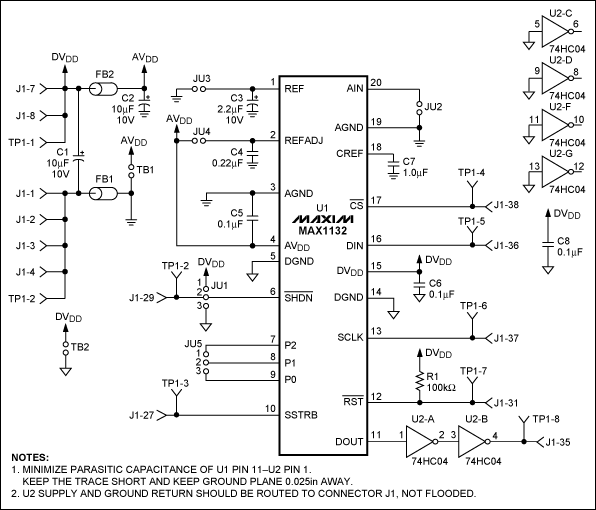
Figure 1. Schematic diagram of the MAX1132 evaluation board
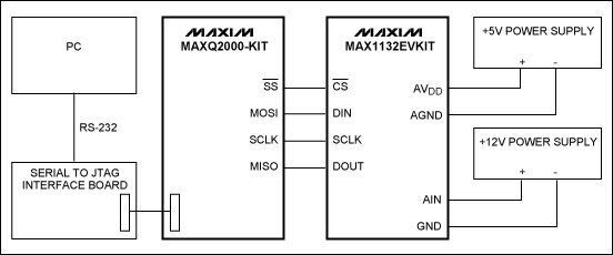
Figure 2. Block diagram of a hardware system for evaluating different SPI clock modes.
The simplest and most flexible SPI clock mode for analysis is the 8-bit mode, because 3 bytes are very suitable for the 24-clock frame format, and the MAX1132 requires exactly 24 clocks to complete the transmission of the data frame. The highest byte sent to the slave is used as the control word (0x80). The highest bit informs the slave to start the conversion, so it is very important (please refer to the MAX1132 data sheet for the control word format). The two low bytes are the data received from the ADC. Ideally, the MAXQ2000's SPI serial clock works at 4MHz, and the ADC's maximum sampling rate should be around 166.67ksps. Table 1 shows the oscilloscope channels assigned to each ADC signal.
Table 1. Oscilloscope channel assignment
In 8-bit mode, the sampling rate of the MAX1132 is approximately 63.7ksps. This rate is lower than the required sampling rate because the serial clock includes the following delays: when SCLK goes high / CS is pulled low, one set of clocks transitions to the next set of clocks, when / CS goes high SCLK is pulled low, and at another time / CS remains high before the start of the adoption (Figure 3).
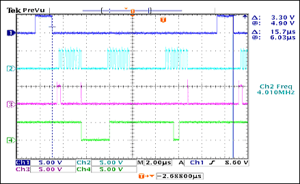
Figure 3. Example of sampling in 8-bit mode
When the SPI clock is in 16-bit mode, two sets of 16 clocks (a total of 32 clocks) are required. The high byte of the first 16 clocks is the control word sent by the microcontroller, and the next byte is the high byte of the data received from the ADC. In the second 16 clocks, the low byte of data is received from the ADC. The remaining 8 clocks in this frame must use the same rate when transmitting continuous data. The sampling rate shown in Figure 4 is 63.7ksps, which is the same as in 8-bit mode.
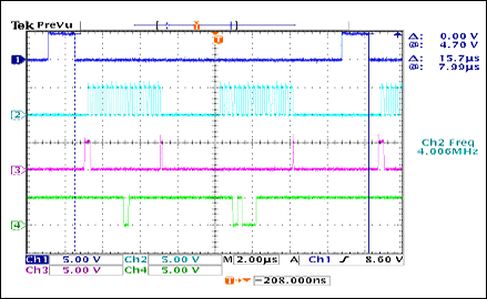
Figure 4. Example of sampling in 16-bit mode
A better method is to first use 8-bit SPI mode to send the control byte, and then switch to 16-bit SPI clock mode to receive the sampled data from the ADC (Figure 5). The advantage of this is that there is no need to divide the data into different clock groups, and no clock cycles are wasted. In combined mode, the sampling rate is 70.4ksps, which is higher than the 8-bit mode and 16-bit mode rate.
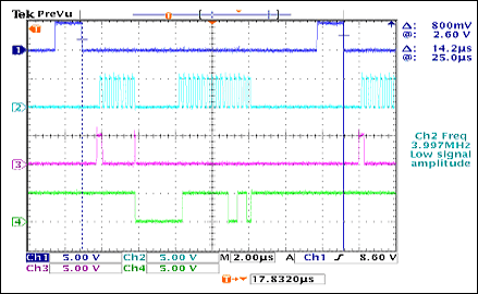
Figure 5. Example of combined mode, that is, the control byte is sent in 8-bit mode, and then the sampled data of the ADC is received in 16-bit mode
In the above example, the collected data can be summarized using the timetable in Table 2. The combined mode is ideal for obtaining the best performance of the MAX1132. This mode uses the least number of clock groups and the least number of single frame clocks. When using 8-bit mode or 16-bit mode respectively, the sampling rate of combined mode cannot be achieved.
Table 2. Delay of a single sampling period in different clock modes
The firmware description C program file (written and compiled in the IAR Embedded Workbench environment for MAXQ) allows the MAXQ2000 SPI interface to communicate with the MAX1132 in a combined mode. When the system clock of MAXQ2000 is 16MHz, the serial clock of SPI is 4MHz.
MAX1132 shows that the MAX1132 is a 200ksps, 16-bit ADC. MAXQ2000 can use different clock modes to interface with MAX1132: including 8-bit, 16-bit, or a combination of both. In order to optimize ADC performance, it is important to decide which mode to adopt at the initial stage of development. Obviously, a 16-bit ADC that includes 16 clock cycles per frame should use 16-bit mode; however, in the specific case where the ADC uses 24 clock cycles per frame, the SPI clock mode must be carefully evaluated. This application note provides test results using 8-bit, 16-bit, and a combination of both. Based on the results, it can be seen that when the MAX1132 uses a 24-clock frame format, the combined mode can be used to obtain the best performance.
Hardware description The application circuit is implemented using the MAX1132 evaluation board and the MAXQ2000 evaluation board.
Figure 1 shows the schematic diagram of the MAX1132 evaluation board, and Figure 2 shows the system configuration diagram. To connect the MAX1132 EV kit to the MAXQ2000 EV kit, connect the SCLK, / CS, DOUT, and DIN pins on the MAX1132 EV kit to the MAXQ2000 EV kit, as shown in Figure 2. In addition, connect a + 5V power supply to the AVDD and AGND ports on the evaluation board. The evaluation board JU1 must be installed in the 1–2 (ON) position. Connect an analog signal of up to + 12V to JU2, and open the other jumpers. To ensure the normal operation of the system, SW3 of the MAXQ2000 evaluation board must be turned off.
Figure 1. Schematic diagram of the MAX1132 evaluation board
Figure 2. Block diagram of a hardware system for evaluating different SPI clock modes.
The simplest and most flexible SPI clock mode for analysis is the 8-bit mode, because 3 bytes are very suitable for the 24-clock frame format, and the MAX1132 requires exactly 24 clocks to complete the transmission of the data frame. The highest byte sent to the slave is used as the control word (0x80). The highest bit informs the slave to start the conversion, so it is very important (please refer to the MAX1132 data sheet for the control word format). The two low bytes are the data received from the ADC. Ideally, the MAXQ2000's SPI serial clock works at 4MHz, and the ADC's maximum sampling rate should be around 166.67ksps. Table 1 shows the oscilloscope channels assigned to each ADC signal.
Table 1. Oscilloscope channel assignment
| Channel | Signal |
| 1 | CS-bar |
| 2 | SCLK |
| 3 | DIN |
| 4 | DOUT |
In 8-bit mode, the sampling rate of the MAX1132 is approximately 63.7ksps. This rate is lower than the required sampling rate because the serial clock includes the following delays: when SCLK goes high / CS is pulled low, one set of clocks transitions to the next set of clocks, when / CS goes high SCLK is pulled low, and at another time / CS remains high before the start of the adoption (Figure 3).
Figure 3. Example of sampling in 8-bit mode
When the SPI clock is in 16-bit mode, two sets of 16 clocks (a total of 32 clocks) are required. The high byte of the first 16 clocks is the control word sent by the microcontroller, and the next byte is the high byte of the data received from the ADC. In the second 16 clocks, the low byte of data is received from the ADC. The remaining 8 clocks in this frame must use the same rate when transmitting continuous data. The sampling rate shown in Figure 4 is 63.7ksps, which is the same as in 8-bit mode.
Figure 4. Example of sampling in 16-bit mode
A better method is to first use 8-bit SPI mode to send the control byte, and then switch to 16-bit SPI clock mode to receive the sampled data from the ADC (Figure 5). The advantage of this is that there is no need to divide the data into different clock groups, and no clock cycles are wasted. In combined mode, the sampling rate is 70.4ksps, which is higher than the 8-bit mode and 16-bit mode rate.
Figure 5. Example of combined mode, that is, the control byte is sent in 8-bit mode, and then the sampled data of the ADC is received in 16-bit mode
In the above example, the collected data can be summarized using the timetable in Table 2. The combined mode is ideal for obtaining the best performance of the MAX1132. This mode uses the least number of clock groups and the least number of single frame clocks. When using 8-bit mode or 16-bit mode respectively, the sampling rate of combined mode cannot be achieved.
Table 2. Delay of a single sampling period in different clock modes
| Interval | Sample TIme, 8-Bit Mode | Sample TIme, 16-Bit Mode | Sample TIme, CombinaTIon Mode |
| CS-bar low to SCLK high | 560ns | 760ns | 960ns |
| Between 1st and 2nd clock sets | 2.32µs | 3.20µs | 2.36µs |
| Between 2nd and 3rd clock sets | 3.12µs | — | — |
| SCLK low to CS-bar high | 2.52µs | 2.60µs | 3.60µs |
| CS-bar high | 1.48µs | 1.44µs | 1.48µs |
| Clock time (1 / SCLK x clocks / frame) | 6.0µs | 8.0µs | 6.0µs |
| Approximate total for one sample | 15.7µs = 63.7ksps | 15.7µs = 63.7ksps | 14.2µs = 70.4ksps |
The firmware description C program file (written and compiled in the IAR Embedded Workbench environment for MAXQ) allows the MAXQ2000 SPI interface to communicate with the MAX1132 in a combined mode. When the system clock of MAXQ2000 is 16MHz, the serial clock of SPI is 4MHz.
6-layer Thick Copper Power Board.with 5OZ copper both (inner&outer). Base material is S1000-2,FR4 tg170. Total board thickness is 2.5 mm. Min. Hole Size 0.3 mm. Min. line width/Min. line spacing 0.3/0.35 mm. surface treatment is Immersion Tin, covered with green solder mask oil. Mixed-Collage board without X-out. 100% E-test.
The industry calls the inner or outer copper thickness equal or greater than 3 oz. The thick copper circuit boards are mainly used in power supply and high power motors. we can provide 1-10 oz thick Copper Circuit Board.

Thick Copper Power Board
Thick Copper Power Board,Heavy Copper PCB,PCB Copper Thickness,PCB Thickness
Orilind Limited Company , https://www.orilind.com