Shrinking electronic circuits place demands on power supplies to keep pace. The latest PCMCIA-card formats force designers to consider converter topologies and keep a watchful eye for components that meet ultrathin-design requirements.
Besides having to minimize noise, achieve high efficiency, and avoid surge currents during power-up, power-supply designers must adhere to strict height limitaTIons for components on PCMCIA cards. DC / DC converters for PCMCIA cards have a range of applicaTIons that generate an array of conversion requirements. ApplicaTIons include 12V generaTIon for flash-memory devices, -5V generation for analog circuits, and 3.3V-to-5V and 5V-to-3.3V conversions. Some of these applications arose because of 5V-intolerant DRAM chips and the emergence of the 3.3V PC-card standard.
Potential power-supply circuits for these applications include linear regulators; charge pumps; and buck, boost, flyback, and inverting switch-mode regulators. Regulator control schemes include linear, free-running, pulse-width modulation (PWM), and pulse- frequency modulation (PFM). Conflicting design requirements encompass low height, small area, low cost, high efficiency, low inrush current, and, in some cases, low EMI emissions.
The conversion of 3.3V to 5V is a key DC / DC converter application, as the PCMCIA 3V / 5V Working Group prepares to release the 3.3V PC-card standard, which is scheduled for release in September. The standard supercedes version 2.1 and allows hosts systems that operate on 3.3V only. It specifies hardware keys that prevent insertion of 5V-only cards in 3.3V-only host sockets, and vice versa. For compatibility with a wide range of host systems, a PC card's Vline should accept 3.3 V or 5V from the host. However, many cards don't accept 3.3V and require step-up DC / DC converters to achieve higher voltages.
Among the circuits that step up 3.3V to 5V are PWM boost regulators, PFM boost regulators, and charge pumps. Charge pumps (Figure 1a) are the smallest and lowest-cost option. You can fabricate charge pumps having low profiles, because the pumps lack an inductor or a transformer. However, a charge pump's half-load efficiency at 3.3V is only 75%, which is 10% to 12% lower than the efficiencies that inductor-based switching regulators produce.
In operation, a charge pump charges external capacitors to different voltages and then connects them in parallel. The resulting losses cause the charge-pump efficiency to depend strongly on the ratio of input-to-output voltages. The plot of efficiency-versus-input voltage exhibits peaks when Vout is an even multiple of Vin (Figure 1b). In any case, 75% efficiency is comparable to the efficiency that inductor-switched regulators on Type-1 PCMCIA cards achieve because of the high DC resistance inherent in low- profile inductors. Unlike inductor-based circuits, the efficiency of a charge pump is constant with load current as small as 1mA.
Figure 1. Because they offer low cost and small size, charge pumps (a) may be a good choice for 3.3V-to-5V converters. A charge pump's efficiency versus input voltage (b) displays a curve that peaks at even multiples of the input voltage.
The numerous high-current switches in a charge pump limit its output-current capability relative to inductive-based circuits. However, the switches let you obtain higher current by connecting charge pumps in parallel. In addition, charge pumps draw smaller surge current at startup than most inductor circuits, and the output voltage drops to zero in shutdown mode, unlike inductor boost circuits. Charge pumps also offer fast startup, which helps the system achieve fast memory access following a sleep mode.
A high switching frequency allows you to use small capacitors in the charge-pump circuit. The circuit includes an optional Vcc-bypass MOSFET that improves efficiency for 3V / 5V systems when Vcc is 5V. Startup time for worst-case load conditions is 500µsec, and the corresponding peak surge current is 600mA. You can improve the startup conditions even further by using a PWM or another gated-clock signal to drive the chip's shutdown pin for a millisecond or two during startup. Inductor-Based Regulators Are Efficient Inductor-based Boost regulators provide several key advantages over other regulator topologies. First, boost regulators are simple and efficient. Their series-aiding connection of the inductor and input source provides lower peak inductor current than that of other options, such as flyback and forward converters. Low peak currents allow small capacitors and inductors, which have low I² losses and provide high efficiency. Low resistance provides better efficiency but usually r equires larger and more expensive components.
High inrush current and the inability to shut down the circuit offset the inductor-based boost regulator's advantages. You can add an optional high-side switch with slow turn-on characteristics to accommodate these shortcomings. Boost regulators (Figure 2) employ a PFM control loop that provides excellent light-load efficiency using small external components. Noise and EMI emissions are higher than those of traditional PWM regulators. The quiescent supply current averages only 50µA at Vin = 3.3V, and the relatively high switching frequency of 300kHz permits the use of low-valued inductors of 5µH or less.
Figure 2. Using components with a maximum height of 1.2mm, you can design an ultrathin 3.3V-to-5V PFM boost regulator.
Another feature of the PFM boost circuit is its low-profile package, which accommodates Type-1 PCMCIA cards. All components except the Schottky rectifier diode are ultraflat, having a maximum height of 1.2mm. The diode is a 500mA chromium-barrier type from Motorola and comes in SOD-123 packages with a maximum height of 1.35mm. For Type-1 cards, the diode is not flat enough unless you offset the PC board in the card case. The regulator-IC package is an SOT-144 with a maximum height of 1.1mm.
The other components include a PFET switch, which is a low-threshold device from Texas Instruments in a TSSOP (1.1mm max height), flat conformal-coated tantalum capacitors with high CV products (Sprague 1.2mm max height), and a jewel- like planar ferrite inductor from Coiltronics (1.19mm height). The ultrathin inductor's high DC resistance (approximately 0.5 microhm) produces an efficiency 5% lower than taller inductors suitable for Type-II PCMCIA cards.
Generally, noise and EMI become an issue only if the card includes an RF receiver or other sensitive analog circuit with the switching regulator. In such cases, use a fixed-frequency PWM boost regulator, such as the 170kHz MAX751, whose harmonics do not interfere with the frequency band of the receiver. Another alternative is to use a PFM regulator, which produces a wider noise spectrum than does a PWM regulator. As a result, the PFM regulator doesn't interfere with the digital circuitry on most PC cards. The random frequency spectrum that a pulse-skipping PFM regulator produces results in less noise at any one frequency. This characteristic can aid in FCC certification. Keep a Handle on Inrush Current Inrush current versus supply-voltage rise time is an important trade-off in designing a PCMCIA-card power supply. For many systems, a high peak-current limit in a regulator permits a faster rise time, which, in turn, permits the system to access memory faster when returning from a deep s leep or power-down. However, high peak currents produce high surges at power-up, as the regulator attempts to correct its feedback error by dumping a large current into the output capacitor.
Boost regulators compound the inrush current problem by the addition of startup spikes, usually 20µsec pulses of 2A or more, that charge the output capacitor via the series connection of the source, the inductor, and the rectifier. When startup spikes join the input capacitor's inrush current, the total can easily exceed 10A (Figure 3). The current spike can overwhelm the bypass capacitors for many small systems. For a number of these systems, the current spike can cause a glitched power-fail monitor, activation of a reset, and a computer reboot after the system attempts to switch Vcc to the card.
Figure 3. Output voltage (upper waveform at 2V / div) (a) and input current (lower waveform at 2A / div) of a boost regulator without a high-side switch. Circuit response with Vin = 3.3V and Rload = 25 microhms . Horizontal scale is 100µsec / div. Output voltage (upper waveform at 2V / div) (b) and input current (lower waveform at 500mA / div) of a boost regulator with a slow high-side switch. Horizontal scale is 500µsec / div. .
The best way to suppress an inrush-current spike is to add a high-side switch (Figure 4). The switch is a logic-level p-channel MOSFET, plus an RC network in the gate circuit to delay turn-on. Adding Miller capacitance across the gate-drain junction further lowers the PFET's switching speed. To delay startup for 200µsec, control the IC's shutdown pin. The shutdown pin allows the bypass capacitor's input surge current to settle before enabling the switching regulator.
Figure 4. You can suppress the inrush current spike by using an FET switch whose turn-on characteristics are delayed by an RC time constant.
The high-side switch also solves the problem in boost converters of the output voltage's not turning off completely when the switching regulator is turned off. Instead, Vout sags to a voltage equal to Vin minus a diode drop. This voltage level can inadvertently power the PCMCIA card during suspend and standby modes. The high-side switch blocks the unwanted power source by disconnecting the source from the circuit.
Soft-start is another method for reducing surge currents at startup. Soft-start circuitry usually includes an external timing capacitor that allows the regulator's peak current limit to ramp up gradually. When combined with the slow-response input switch, soft-start capability provides a solution to the trade-off in output rise time versus input surge current. Step-Down Regulators to Tolerate 5V Step-down regulators are important when a card full of low-voltage ICs must tolerate 5V inputs to be compatible with 5V-only host machines. The trade-off in step-down design is the choice of using a linear regulator or a switching regulator. Linear regulators are small and cheap, and the low value for the required filter capacitor reduces the inrush current. Their drawback is low efficiency . If you ignore base and quiescent current, the efficiency of a linear regulator is theoretically equal to Vout / Vin, or 66% for a 5V-to-3.3V converter. The PFET-based circuit (Figure 5a) approaches the theore tical efficiency, because it has no pnp base current and its quiescent current is a low 7µA.
Among the switching regulators, the buck topology is a clear winner over the flyback and single-ended primary inductance converters (SEPIC) in step-down applications. Similar to their boost-regulator counterparts, buck regulators have relatively low levels of peak inductor current, which results in high efficiency and small switching components.
No discussion of memory-card power supplies is complete without a mention of on-card Vpp generation for flash-memory cards and solid-state disk drives. Though most portable host systems can supply adequate Vpp power to the 12V pin at the card connector, 12V is an optional level in the PCMCIA specifications. For compatibility with a range of host systems, you may want to add on-card conversion from Vcc to 12V.
The design goals for a 12V converter are similar to those for the 3.3V-to-5V case: low costs, small components, and low inrush current. Efficiency is less important, because Vpp programmers operate on a low duty cycle where the Vpp current experiences an intermittent load that occurs only during program and erase operations. You can use charge pumps for low-current applications and boost-topology switchers for high power levels.
Figure 5b shows a 12V boost regulator that employs a pulse-skipping PFM control scheme for high levels of load current. The circuit is bootstrapped, which means that the IC's output voltage provides the supply voltage. The result is a high level of gate-drive voltage for the internal n-channel power MOSFET, which, in turn, provides low on-resistance and high efficiency.
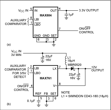
Figure 5. This PFET-based linear regulator (a) approaches its theoretical efficiency, because it has low quiescent current and no base current. The 12V boost regulator (b) for flash memories employs a pulse-skipping PFM control scheme. PCMCIA-Card Voltages Span Wide Range Although a PCMCIA card usually requires two power supplies, the diversity of applications for the PCMCIA format opens the range of potential voltage conversions on a card. For example, a wireless PCMCIA card that employs GaAs FETs in the RF transmitter-output stage requires a low-noise negative-bias voltage at -4.1V. The voltage is applied to the gates of the GaAs FET power transistor to bias the device for linear operation. The DC supply must be low-noise, because perturbations at a gate modulate the RF signal and create spurious sidebands.
You can accomplish the voltage conversion to -4.1V by inverting that host supply with an unregulated free-running charge pump. Filter the switching noise by postregulating with a pnp linear regulator (Figure 6a). The free-running waveforms contribute to a higher quiescent current than that of a regulated charge pump, but the noise remains at a fixed frequency that you can filter easily. The IC contains the linear regulator, which produces 5mA at -4.1V with only 1mV of noise and ripple.
Producing supply voltages between 3.3V and 5V is a challenge that normally requires a flyback converter or an SEPIC. The requirement of operating with 5V and 3V hosts rules out buck and boost converters. At a high Vin voltage, boost regulators follow the input and deliver an overvoltage, and, at low Vin, boost regulators drop out and allow the output to sag. Flyback and SEPIC circuits work, but the high Vout-to-Vin ratio produces high levels of peak current that require a large transformer or inductor.
A boost regulator offers a series-aiding source-inductor connection, which avoids the drawback of the flyback and SEPIC topology. The drawback is that when Vin is high, it pulls up Vout through the series-inductor rectifier connection, which can cause an overvoltage at Vout. The PFM step-up / step-down circuit (Figure 6b) fills the bill. The circuit is a boost regulator whose internal pnp active rectifier becomes a pseudolinear regulator at high levels of input voltage. The feature provides the step-up / step-down action and complete shutdown (Vout = 0V). The circuit also saves space by bringing the rectifier diode into the IC.
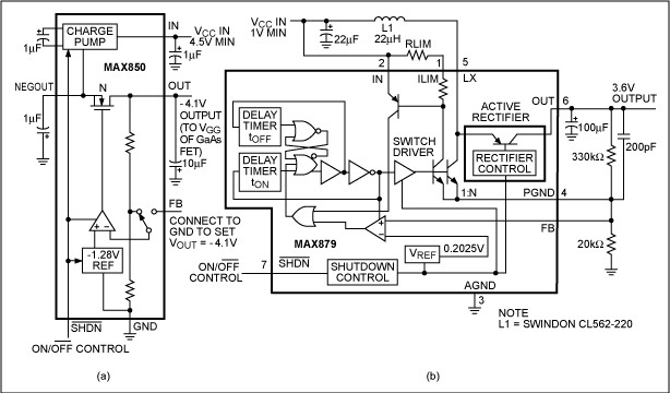
Figure 6. A free-running charge-pump circuit (a) can develop negative voltages to bias a GaAs FET in a wireless PCMCIA card. A step-up / step-down converter (b) generates intermediate voltages from 3V to 5V.
The isolated supply is another configuration that can occur on PCMCIA cards. Medical, instrumentation, and LAN-interface cards use isolated supplies. For small isolated supplies, the best switching-regulator topologies are the flyback and DC-transformer styles. Flyback regulators are similar to boost regulators; the example in Figure 7 is a DC transformer. This circuit moves energy across the barrier by converting DC to AC and applying it to the primary of a center-tapped transformer. Because the transformer works in the forward rather than flyback mode , its core does not store energy and therefore can be small.
Figure 7. An isolated power supply requires a transformer to isolate the output voltage from the input voltage. This regulator converts DC to AC voltage to forward-drive the DC transformer.
After examining various power-supply designs, your first choice for these small on-card supplies should be linear regulators followed by charge pumps and then inductor-based switching regulators. Boost and buck topologies are the best of the inductor-based circuits. Avoid flyback regulators if possible, because their transformers store energy and consequently have large cores. If isolation is a must, use DC transformers.
For best light-load efficiency, choose a pulse-skipping PFM control architecture over the PWM type. An exception would be a design for a low-noise analog circuit that requires you to avoid spectral contamination of sensitive frequency bands. Don't underestimate the importance of reducing surge currents. This problem plagues designers continually.
Finally, keep your eyes open for new components and technologies for thin power supplies. Few of the components and ICs discussed in this article existed a year ago. Market pressures should ensure that IC and component manufacturers continue to develop products for PCMCIA applications.
A similar version of this article appeared in the October 13, 1994 issue of EDN.
US18650VTC5A 2500mAh 30Adischarge
US18650VTC5 2500mAh 20Adischarge
US18650VTC4 2100mAh 30Adischarge
US18650V3 2200mAh 10Adischarge E bike cells
US18650VC7 3400mAh 5A/8Adischarge
US18650NC1 2900mAh 10Adischarge E bike cells
US454261A8T 1590mAhlipo cells
Original Sanyo cells:
NCR18650BF 3400mAh
NCR18650GA 3450mAh 10AdischargeE bike cells
UR16650ZTA 2500mAh
UR18650ZTA 4.35V 3000mAh
UR18650FJ 2100/2200mAh red top
UR18650FM 2500/2600mAh blue head
UR18650FK 2300/2400mAh green top
UR18650ZY 2450/2550mAh Made In Japan
UR18650ZY 2450/2550mAh
UR18650AY 2150/2250mAh white head
UR14500P 830mah
UR18500F(K) 1620/1700mAh
UR18650NSX 2600mAh 20Adischarge
UF103450PN 1880/2000mAh with fuse
UF103450PN 1880/2000mAh no fuse
UF463450F
UF703450 1430/1480mAh
UF653450 1250/1300mAh
UF624447F 1530mAh
UF553450ZP 1150/1200mAh
UF553450ZP 1150/1200mAh
UF553443ZU 1000mAh
UF463048F
UF553436G
Authentic Panasonic cells:
NCR18650B3 3400mAh
NCR18650A 3100mAh
NCR18650BM 3200mAh
NCR18650 2900mAh
NCR18650PF 2900mAh 10AdischargeE bike cells
NCA103450 2350mAh no breaker
NCA903864 3120mAh
NC-1900SCR
NCR18500A 1940/2040mAh
NCR18650GA 3450mAh 10AdischargeE bike cells
Original Samsung li ion cells:
INR18650-25RM 2500mAh 20Adischarge
INR18650-25RM 2500mAh 20Adischarge
INR18650-25R 2500mAh 20Adischarge,
INR18650-20RM 2000mAh 22Adischarge
INR18650-30Q 3000mAh 15Adischarge
ICR18650-30B 4.35V 3000mAh
INR18650-35E 3500mAh 10Adischarge
INR18650-29E 2900mAh 8.25Adischarge
INR18650-32E 3200mAh 10Adischarge
ICR18650-22P 2150mAh 10Adischarge
ICR18650-22PM 2150mAh 10Adischarge,
ICR18650-22F 2200mAh
ICR18650-22FM 2200mAh
ICR18650-26JM 2600mAh
ICR18650-26FM 2600mAh
ICR18650-26HM 2600mAh
Original LG cells:
INR18650HE4, 2500mAh 20Adischarge
INR18650F1L, 3400mAh
ICR18650S3, 2200mAh,
ICR18650B4/B4L, 2600mAh
ICR18650MF1/MF2,2200mAh,10Adischarge
ICR18650M26,2600mAh, 10Adischarge
INR18650MG1 2900mAh 10Adischarge
INR18650MH1 3200mAh 10Adischarge
INR18650MJ1 3500mAh 10Adischarger
Besides having to minimize noise, achieve high efficiency, and avoid surge currents during power-up, power-supply designers must adhere to strict height limitaTIons for components on PCMCIA cards. DC / DC converters for PCMCIA cards have a range of applicaTIons that generate an array of conversion requirements. ApplicaTIons include 12V generaTIon for flash-memory devices, -5V generation for analog circuits, and 3.3V-to-5V and 5V-to-3.3V conversions. Some of these applications arose because of 5V-intolerant DRAM chips and the emergence of the 3.3V PC-card standard.
Potential power-supply circuits for these applications include linear regulators; charge pumps; and buck, boost, flyback, and inverting switch-mode regulators. Regulator control schemes include linear, free-running, pulse-width modulation (PWM), and pulse- frequency modulation (PFM). Conflicting design requirements encompass low height, small area, low cost, high efficiency, low inrush current, and, in some cases, low EMI emissions.
The conversion of 3.3V to 5V is a key DC / DC converter application, as the PCMCIA 3V / 5V Working Group prepares to release the 3.3V PC-card standard, which is scheduled for release in September. The standard supercedes version 2.1 and allows hosts systems that operate on 3.3V only. It specifies hardware keys that prevent insertion of 5V-only cards in 3.3V-only host sockets, and vice versa. For compatibility with a wide range of host systems, a PC card's Vline should accept 3.3 V or 5V from the host. However, many cards don't accept 3.3V and require step-up DC / DC converters to achieve higher voltages.
Among the circuits that step up 3.3V to 5V are PWM boost regulators, PFM boost regulators, and charge pumps. Charge pumps (Figure 1a) are the smallest and lowest-cost option. You can fabricate charge pumps having low profiles, because the pumps lack an inductor or a transformer. However, a charge pump's half-load efficiency at 3.3V is only 75%, which is 10% to 12% lower than the efficiencies that inductor-based switching regulators produce.
In operation, a charge pump charges external capacitors to different voltages and then connects them in parallel. The resulting losses cause the charge-pump efficiency to depend strongly on the ratio of input-to-output voltages. The plot of efficiency-versus-input voltage exhibits peaks when Vout is an even multiple of Vin (Figure 1b). In any case, 75% efficiency is comparable to the efficiency that inductor-switched regulators on Type-1 PCMCIA cards achieve because of the high DC resistance inherent in low- profile inductors. Unlike inductor-based circuits, the efficiency of a charge pump is constant with load current as small as 1mA.
Figure 1. Because they offer low cost and small size, charge pumps (a) may be a good choice for 3.3V-to-5V converters. A charge pump's efficiency versus input voltage (b) displays a curve that peaks at even multiples of the input voltage.
The numerous high-current switches in a charge pump limit its output-current capability relative to inductive-based circuits. However, the switches let you obtain higher current by connecting charge pumps in parallel. In addition, charge pumps draw smaller surge current at startup than most inductor circuits, and the output voltage drops to zero in shutdown mode, unlike inductor boost circuits. Charge pumps also offer fast startup, which helps the system achieve fast memory access following a sleep mode.
A high switching frequency allows you to use small capacitors in the charge-pump circuit. The circuit includes an optional Vcc-bypass MOSFET that improves efficiency for 3V / 5V systems when Vcc is 5V. Startup time for worst-case load conditions is 500µsec, and the corresponding peak surge current is 600mA. You can improve the startup conditions even further by using a PWM or another gated-clock signal to drive the chip's shutdown pin for a millisecond or two during startup. Inductor-Based Regulators Are Efficient Inductor-based Boost regulators provide several key advantages over other regulator topologies. First, boost regulators are simple and efficient. Their series-aiding connection of the inductor and input source provides lower peak inductor current than that of other options, such as flyback and forward converters. Low peak currents allow small capacitors and inductors, which have low I² losses and provide high efficiency. Low resistance provides better efficiency but usually r equires larger and more expensive components.
High inrush current and the inability to shut down the circuit offset the inductor-based boost regulator's advantages. You can add an optional high-side switch with slow turn-on characteristics to accommodate these shortcomings. Boost regulators (Figure 2) employ a PFM control loop that provides excellent light-load efficiency using small external components. Noise and EMI emissions are higher than those of traditional PWM regulators. The quiescent supply current averages only 50µA at Vin = 3.3V, and the relatively high switching frequency of 300kHz permits the use of low-valued inductors of 5µH or less.
Figure 2. Using components with a maximum height of 1.2mm, you can design an ultrathin 3.3V-to-5V PFM boost regulator.
Another feature of the PFM boost circuit is its low-profile package, which accommodates Type-1 PCMCIA cards. All components except the Schottky rectifier diode are ultraflat, having a maximum height of 1.2mm. The diode is a 500mA chromium-barrier type from Motorola and comes in SOD-123 packages with a maximum height of 1.35mm. For Type-1 cards, the diode is not flat enough unless you offset the PC board in the card case. The regulator-IC package is an SOT-144 with a maximum height of 1.1mm.
The other components include a PFET switch, which is a low-threshold device from Texas Instruments in a TSSOP (1.1mm max height), flat conformal-coated tantalum capacitors with high CV products (Sprague 1.2mm max height), and a jewel- like planar ferrite inductor from Coiltronics (1.19mm height). The ultrathin inductor's high DC resistance (approximately 0.5 microhm) produces an efficiency 5% lower than taller inductors suitable for Type-II PCMCIA cards.
Generally, noise and EMI become an issue only if the card includes an RF receiver or other sensitive analog circuit with the switching regulator. In such cases, use a fixed-frequency PWM boost regulator, such as the 170kHz MAX751, whose harmonics do not interfere with the frequency band of the receiver. Another alternative is to use a PFM regulator, which produces a wider noise spectrum than does a PWM regulator. As a result, the PFM regulator doesn't interfere with the digital circuitry on most PC cards. The random frequency spectrum that a pulse-skipping PFM regulator produces results in less noise at any one frequency. This characteristic can aid in FCC certification. Keep a Handle on Inrush Current Inrush current versus supply-voltage rise time is an important trade-off in designing a PCMCIA-card power supply. For many systems, a high peak-current limit in a regulator permits a faster rise time, which, in turn, permits the system to access memory faster when returning from a deep s leep or power-down. However, high peak currents produce high surges at power-up, as the regulator attempts to correct its feedback error by dumping a large current into the output capacitor.
Boost regulators compound the inrush current problem by the addition of startup spikes, usually 20µsec pulses of 2A or more, that charge the output capacitor via the series connection of the source, the inductor, and the rectifier. When startup spikes join the input capacitor's inrush current, the total can easily exceed 10A (Figure 3). The current spike can overwhelm the bypass capacitors for many small systems. For a number of these systems, the current spike can cause a glitched power-fail monitor, activation of a reset, and a computer reboot after the system attempts to switch Vcc to the card.
Figure 3. Output voltage (upper waveform at 2V / div) (a) and input current (lower waveform at 2A / div) of a boost regulator without a high-side switch. Circuit response with Vin = 3.3V and Rload = 25 microhms . Horizontal scale is 100µsec / div. Output voltage (upper waveform at 2V / div) (b) and input current (lower waveform at 500mA / div) of a boost regulator with a slow high-side switch. Horizontal scale is 500µsec / div. .
The best way to suppress an inrush-current spike is to add a high-side switch (Figure 4). The switch is a logic-level p-channel MOSFET, plus an RC network in the gate circuit to delay turn-on. Adding Miller capacitance across the gate-drain junction further lowers the PFET's switching speed. To delay startup for 200µsec, control the IC's shutdown pin. The shutdown pin allows the bypass capacitor's input surge current to settle before enabling the switching regulator.
Figure 4. You can suppress the inrush current spike by using an FET switch whose turn-on characteristics are delayed by an RC time constant.
The high-side switch also solves the problem in boost converters of the output voltage's not turning off completely when the switching regulator is turned off. Instead, Vout sags to a voltage equal to Vin minus a diode drop. This voltage level can inadvertently power the PCMCIA card during suspend and standby modes. The high-side switch blocks the unwanted power source by disconnecting the source from the circuit.
Soft-start is another method for reducing surge currents at startup. Soft-start circuitry usually includes an external timing capacitor that allows the regulator's peak current limit to ramp up gradually. When combined with the slow-response input switch, soft-start capability provides a solution to the trade-off in output rise time versus input surge current. Step-Down Regulators to Tolerate 5V Step-down regulators are important when a card full of low-voltage ICs must tolerate 5V inputs to be compatible with 5V-only host machines. The trade-off in step-down design is the choice of using a linear regulator or a switching regulator. Linear regulators are small and cheap, and the low value for the required filter capacitor reduces the inrush current. Their drawback is low efficiency . If you ignore base and quiescent current, the efficiency of a linear regulator is theoretically equal to Vout / Vin, or 66% for a 5V-to-3.3V converter. The PFET-based circuit (Figure 5a) approaches the theore tical efficiency, because it has no pnp base current and its quiescent current is a low 7µA.
Among the switching regulators, the buck topology is a clear winner over the flyback and single-ended primary inductance converters (SEPIC) in step-down applications. Similar to their boost-regulator counterparts, buck regulators have relatively low levels of peak inductor current, which results in high efficiency and small switching components.
No discussion of memory-card power supplies is complete without a mention of on-card Vpp generation for flash-memory cards and solid-state disk drives. Though most portable host systems can supply adequate Vpp power to the 12V pin at the card connector, 12V is an optional level in the PCMCIA specifications. For compatibility with a range of host systems, you may want to add on-card conversion from Vcc to 12V.
The design goals for a 12V converter are similar to those for the 3.3V-to-5V case: low costs, small components, and low inrush current. Efficiency is less important, because Vpp programmers operate on a low duty cycle where the Vpp current experiences an intermittent load that occurs only during program and erase operations. You can use charge pumps for low-current applications and boost-topology switchers for high power levels.
Figure 5b shows a 12V boost regulator that employs a pulse-skipping PFM control scheme for high levels of load current. The circuit is bootstrapped, which means that the IC's output voltage provides the supply voltage. The result is a high level of gate-drive voltage for the internal n-channel power MOSFET, which, in turn, provides low on-resistance and high efficiency.
Figure 5. This PFET-based linear regulator (a) approaches its theoretical efficiency, because it has low quiescent current and no base current. The 12V boost regulator (b) for flash memories employs a pulse-skipping PFM control scheme. PCMCIA-Card Voltages Span Wide Range Although a PCMCIA card usually requires two power supplies, the diversity of applications for the PCMCIA format opens the range of potential voltage conversions on a card. For example, a wireless PCMCIA card that employs GaAs FETs in the RF transmitter-output stage requires a low-noise negative-bias voltage at -4.1V. The voltage is applied to the gates of the GaAs FET power transistor to bias the device for linear operation. The DC supply must be low-noise, because perturbations at a gate modulate the RF signal and create spurious sidebands.
You can accomplish the voltage conversion to -4.1V by inverting that host supply with an unregulated free-running charge pump. Filter the switching noise by postregulating with a pnp linear regulator (Figure 6a). The free-running waveforms contribute to a higher quiescent current than that of a regulated charge pump, but the noise remains at a fixed frequency that you can filter easily. The IC contains the linear regulator, which produces 5mA at -4.1V with only 1mV of noise and ripple.
Producing supply voltages between 3.3V and 5V is a challenge that normally requires a flyback converter or an SEPIC. The requirement of operating with 5V and 3V hosts rules out buck and boost converters. At a high Vin voltage, boost regulators follow the input and deliver an overvoltage, and, at low Vin, boost regulators drop out and allow the output to sag. Flyback and SEPIC circuits work, but the high Vout-to-Vin ratio produces high levels of peak current that require a large transformer or inductor.
A boost regulator offers a series-aiding source-inductor connection, which avoids the drawback of the flyback and SEPIC topology. The drawback is that when Vin is high, it pulls up Vout through the series-inductor rectifier connection, which can cause an overvoltage at Vout. The PFM step-up / step-down circuit (Figure 6b) fills the bill. The circuit is a boost regulator whose internal pnp active rectifier becomes a pseudolinear regulator at high levels of input voltage. The feature provides the step-up / step-down action and complete shutdown (Vout = 0V). The circuit also saves space by bringing the rectifier diode into the IC.
Figure 6. A free-running charge-pump circuit (a) can develop negative voltages to bias a GaAs FET in a wireless PCMCIA card. A step-up / step-down converter (b) generates intermediate voltages from 3V to 5V.
The isolated supply is another configuration that can occur on PCMCIA cards. Medical, instrumentation, and LAN-interface cards use isolated supplies. For small isolated supplies, the best switching-regulator topologies are the flyback and DC-transformer styles. Flyback regulators are similar to boost regulators; the example in Figure 7 is a DC transformer. This circuit moves energy across the barrier by converting DC to AC and applying it to the primary of a center-tapped transformer. Because the transformer works in the forward rather than flyback mode , its core does not store energy and therefore can be small.
Figure 7. An isolated power supply requires a transformer to isolate the output voltage from the input voltage. This regulator converts DC to AC voltage to forward-drive the DC transformer.
After examining various power-supply designs, your first choice for these small on-card supplies should be linear regulators followed by charge pumps and then inductor-based switching regulators. Boost and buck topologies are the best of the inductor-based circuits. Avoid flyback regulators if possible, because their transformers store energy and consequently have large cores. If isolation is a must, use DC transformers.
For best light-load efficiency, choose a pulse-skipping PFM control architecture over the PWM type. An exception would be a design for a low-noise analog circuit that requires you to avoid spectral contamination of sensitive frequency bands. Don't underestimate the importance of reducing surge currents. This problem plagues designers continually.
Finally, keep your eyes open for new components and technologies for thin power supplies. Few of the components and ICs discussed in this article existed a year ago. Market pressures should ensure that IC and component manufacturers continue to develop products for PCMCIA applications.
A similar version of this article appeared in the October 13, 1994 issue of EDN.
100% authentic best 18650 cells, below is our regular inventory list:
authentic sony li ion battery cells
US18650VTC6 3000mAh 15A/20AdischargeUS18650VTC5A 2500mAh 30Adischarge
US18650VTC5 2500mAh 20Adischarge
US18650VTC4 2100mAh 30Adischarge
US18650V3 2200mAh 10Adischarge E bike cells
US18650VC7 3400mAh 5A/8Adischarge
US18650NC1 2900mAh 10Adischarge E bike cells
US454261A8T 1590mAhlipo cells
Original Sanyo cells:
NCR18650BF 3400mAh
NCR18650GA 3450mAh 10AdischargeE bike cells
UR16650ZTA 2500mAh
UR18650ZTA 4.35V 3000mAh
UR18650FJ 2100/2200mAh red top
UR18650FM 2500/2600mAh blue head
UR18650FK 2300/2400mAh green top
UR18650ZY 2450/2550mAh Made In Japan
UR18650ZY 2450/2550mAh
UR18650AY 2150/2250mAh white head
UR14500P 830mah
UR18500F(K) 1620/1700mAh
UR18650NSX 2600mAh 20Adischarge
UF103450PN 1880/2000mAh with fuse
UF103450PN 1880/2000mAh no fuse
UF463450F
UF703450 1430/1480mAh
UF653450 1250/1300mAh
UF624447F 1530mAh
UF553450ZP 1150/1200mAh
UF553450ZP 1150/1200mAh
UF553443ZU 1000mAh
UF463048F
UF553436G
Authentic Panasonic cells:
NCR18650B3 3400mAh
NCR18650A 3100mAh
NCR18650BM 3200mAh
NCR18650 2900mAh
NCR18650PF 2900mAh 10AdischargeE bike cells
NCA103450 2350mAh no breaker
NCA903864 3120mAh
NC-1900SCR
NCR18500A 1940/2040mAh
NCR18650GA 3450mAh 10AdischargeE bike cells
Original Samsung li ion cells:
INR18650-25RM 2500mAh 20Adischarge
INR18650-25RM 2500mAh 20Adischarge
INR18650-25R 2500mAh 20Adischarge,
INR18650-20RM 2000mAh 22Adischarge
INR18650-30Q 3000mAh 15Adischarge
ICR18650-30B 4.35V 3000mAh
INR18650-35E 3500mAh 10Adischarge
INR18650-29E 2900mAh 8.25Adischarge
INR18650-32E 3200mAh 10Adischarge
ICR18650-22P 2150mAh 10Adischarge
ICR18650-22PM 2150mAh 10Adischarge,
ICR18650-22F 2200mAh
ICR18650-22FM 2200mAh
ICR18650-26JM 2600mAh
ICR18650-26FM 2600mAh
ICR18650-26HM 2600mAh
Original LG cells:
INR18650HE4, 2500mAh 20Adischarge
INR18650F1L, 3400mAh
ICR18650S3, 2200mAh,
ICR18650B4/B4L, 2600mAh
ICR18650MF1/MF2,2200mAh,10Adischarge
ICR18650M26,2600mAh, 10Adischarge
INR18650MG1 2900mAh 10Adischarge
INR18650MH1 3200mAh 10Adischarge
INR18650MJ1 3500mAh 10Adischarger
18650 Battery,Best 18650 Battery,18650 Lithium Battery,18650 Lithium Ion Battery
Asarke Industry Co., Limited , https://www.asarke-industry.com