
Tencent Digital (Compiled: Mike) There are currently about 1.4 billion people in the world living in an environment without electricity or streetlights. People in many places face dark environments at night, which leads to more dangers and crimes. The occurrence of the incident.
And if people in these impoverished and developing regions can also use street lights and electric energy, it will be a good thing for the benefit of mankind. Clean energy is the best choice for people in these poor areas to use electricity.
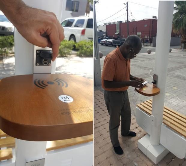
There is now a very interesting smart streetlight project, the InGogolago, on Indiegogo. This streetlight can not only absorb solar energy from the top solar panel, but also can convert the human footsteps around it into electrical energy.

Surrounding this type of EnGoPlanet smart streetlight, there is an accompanying conversion pedal, and when someone steps on the pedal, about 7w of electricity is generated, which is stored in the streetlight's battery. This kind of street lamp is very suitable for installation in some countries and regions in Africa.
And this kind of street light has one kind of advantage that it is quite environmentally friendly. We must know that there are more than 300 million street lights in the world, the annual operating cost exceeds 40 billion US dollars, and more than 100 million tons of carbon dioxide are released, and global warming is also made. Your own "contribution." The EnGoPlanet street light can use clean energy and bring lighting to people in poor areas, shouldering the task of changing the world.

In addition to the built-in battery to conserve the power of the solar and ground pedals, each EnGoPlanet can provide free Wi-Fi signals and can also function as a mobile charging station. Even sensors can be used in the future to monitor air quality, temperature, humidity, and other information.

How, if you can really make this kind of EnGoPlanet smart street lamp popular, can it not only bring people nightlight in the poor areas, but also make more contribution to reducing carbon dioxide emissions.
At present, the EnGoPlanet smart streetlight has started crowdfunding on Indiegogo with a crowdfunding target of US$300,000. The early bird price is US$5,000 (approximately RMB33,800), and if all goes well, it is expected to begin testing in February 2017. Interested friends may wish to rush to support it.
Source: indiegogo
HDI PCB Specification
High density interconnect (HDI) PCBs represent one of the fastest-growing segments of the printed circuit board market. Because of its higher circuitry density, the HDI PCB design is able to incorporate finer lines and spaces, smaller vias and capture pads, and higher connection pad densities. A high density PCB features blind and buried vias and often contains microvias that are .006 in diameter or even less.
HDI PCBs are characterized by high-density attributes including laser microvias, fine lines and high performance thin materials. This increased density enables more functions per unit area. Higher technology HDI PCBs have multiple layers of copper filled stacked microvias (Advanced HDI PCBs) which creates a structure that enables even more complex interconnections. These very complex structures provide the necessary routing solutions for today's large pin-count chips utilized in mobile devices and other high technology products.
The HDI PCBs we offer include the following highly requested characteristics:
Blind and/or buried vias
Via-in-pad
Through vias from surface to surface
20 µm circuit geometries
30 µm dielectric layers
50 µm laser vias
125 µm bump pitch processing
Applications
HDI PCB is used to reduce size and weight, as well as to enhance electrical performance of the device. HDI PCB is the best alternative to high layer-count and expensive standard laminate or sequentially laminated boards. HDI incorporate blind and buried vias that help to save PCB real estate by allowing features and lines to be designed above or below them without making a connection. Many of today's fine pitch BGA and flip-chip component footprints do not allow for running traces between the BGA pads. Blind and buried vias will only connect layers requiring connections in that area.
HDI PCB,Special HDI PCB,HDI Prototype PCB,HDI Board PCB
Storm Circuit Technology Ltd , https://www.stormpcb.com