At present, many manufacturers provide universal serial communication chips, and their transmission methods are divided into synchronous and asynchronous modes. Among them, asynchronous chips are mostly compatible with INTEL's 8250 chip; while the synchronous mode generally involves the supported transmission protocols (BSC, HDLC, SDLC, etc.), so when users require the application of specific synchronous transmission protocols, they often need to design special SRT (Synchronous Transceiver). In the past, most common logic components were used for design, which led to a lengthy design and debugging process and low system stability, which was very inconvenient. Nowadays, as the programmable ASIC technology represented by FPGA and CPLD becomes more mature and perfect, users can use EDA technology as a development method according to their own requirements, and use a FPGA or CPLD to design a chip that meets their needs. This article takes the development of a dedicated synchronous transceiver chip in a statistical time-division multiplexer as an example to introduce the development process of the entire chip.
1 Statistical time division multiplexer system functions and module composition
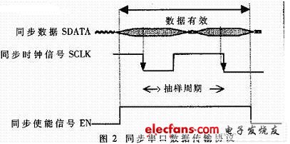
The statistical time division multiplexer completes the multiplexing of 7 asynchronous data and 1 synchronous data. Its functional block diagram is shown in Figure 1, and the synchronous serial port transmission protocol is shown in Figure 2. Due to the short transmission distance and the small number of channels, the function is relatively simple. For system power consumption and cost considerations, this dedicated SRT and the entire interface control unit are integrated into a CPLD (XC95144).

2 CPLD internal functional block diagram and design
The internal structure of CPLD is mainly composed of interface control unit and SRT. Here we mainly introduce the structure and function module of SRT (see Figure 3). Because the selected UART (Universal Asynchronous Transceiver) is compatible with INS8250, in order to simplify the programming of the main control unit to access the external communication chip, the operation flow is unified, and the structure of SRT is imitated as much as possible in the design of SRT.

This design uses a modular design. According to the function, the internal structure of SRT is divided into 5 modules, and each module corresponds to a VHDL design file. The advantage of this design is that it is conducive to the writing and debugging of each functional module, thereby reducing the debugging difficulty of the entire SRT and improving the maintainability and readability of the software. The following is a brief introduction of the external functions of each design file (port description and some implementation codes are listed for several important modules):
(1) SRTCRTL.VHD
SRTCRTL.VHD, as the SRT control module, is responsible for address decoding. When the chip select signal is valid, the data on the data line is written to the corresponding register. The SRT chip has a total of 6 control registers including a receive buffer, a transmission holder, a line control register, a divisor register (one for each of the high and low 8 bits), and a loop control register. Each register is assigned an address. By reading and writing the corresponding address, the CPU can complete operations such as data sending, receiving, self-loop and chip parameter setting.
(2) LOOP.VHD
The function of this module is to test the function of the chip itself according to the user's instructions. The user first sets the chip to the self-loop state, so that the internal transmission data line of the chip is short-circuited with the direct reception data line; then, by writing specific data to the transmission holder, it is compared with the data read from the reception buffer. If they are the same, the user can judge whether the chip is working properly.
(3) CLKGEN.VHD
CLKGEN.VHD is a baud rate generator module, which is used to generate the synchronous clock signal doclk. It divides the 8-bit and 16-bit data of the divisor register as a divisor and divides the external 2MHz clock source. The user can dynamically change the data transmission rate by modifying the value of the divisor register, so the operation is convenient and flexible.
(4) RBR.VHD
RR.VHD as the receiving module of the whole chip, including receiving buffer, receiving data synchronization, serial / parallel conversion.
The port description is as follows:
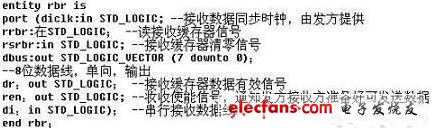
When there is no data in the receive buffer, the ren signal is valid to notify the sender to transmit the data. Then sample the di signal according to dilck, once the buffer is full, ren is invalid, dr is valid, and the CPU is notified to read.
Nickel Alkaline Battery,Solar Energy Battery,48V Nife Battery 200Ah ,Ni-Fe Battery 100~200Ah
Henan Xintaihang Power Source Co.,Ltd , https://www.taihangbattery.com