Audio amplifier circuit diagram:
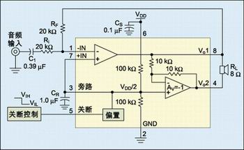
This is a typical application circuit for audio power amplifiers. It is limited by design and cannot work in a high-circuit noise environment. Increasing the bypass capacitor value can improve the power supply rejection ratio. However, if the value of the bypass capacitor is high, the turn-on time may be prolonged and the volume of the capacitor increases, which is not practical.
Figure II:
This is an application circuit for audio power amplifiers with the function of "increasing gradually weakening". It adds the function of “gradually weakening graduallyâ€. When the LM4897 amplifier receives power from the shutdown pin and restarts, the output level will slowly rise. After receiving the stop signal, the output level will gradually drop to zero, and the start / stop time can be set by the input resistance and capacitor.
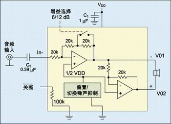
Figure 3:
This is an audio amplifier that uses no bypass capacitors. Without the bypass capacitor, the startup time can be shortened, and the power supply rejection ratio of up to 62dB and 66dB can be maintained under the noise of 217Hz and 1kHz, respectively. The audio amplifier has built-in input and feedback resistors. Engineers can use external control logic pins to select 2x (6dB) or 4x (12dB) programmable gain. The number of external components can be greatly reduced to two.
OPGW Cable Fittings Manufacturers, OPGW Cable Fittings Suppliers, China OPGW Cable Fittings, Cable Fittings,Opgw Cable Fittings,Opgw Fiber Optic Cable,Vibration Damper For Opgw
Shandong Qingguo Optical Fiber Co., Ltd. , https://www.qgfiber.com