This article describes a high power factor flyback converter for LED illumination that implements all of these features and enables dimming using a standard thyristor (TRIAC) based dimmer.
I. Counterattack foundation
For isolated power supplies up to about 100W, the flyback topology has been widely accepted because it is relatively simple, has fewer components, is cost effective, and has reasonable performance. With Fairchild Semiconductor Application Note AN-4137, the basic working principle is simple and easy to explain. When MOSFET Q1 is turned on, the current in the primary side of transformer T1 ramps up linearly, creating a magnetic field that stores energy. The polarity of the transformer winding shows that the polarity meets the condition so that the secondary rectifier DRect turns off during this period. Once the MOSFET is turned off, the polarity of all voltages across the transformer is reversed according to Lenz's law. The DRect is now turned on and the energy stored in T1 is transferred to the capacitor CFilt. The duty cycle of the PWM controller, together with the transformer turn ratio, determines the output voltage, which is stable with the help of an isolated feedback network. Due to the incomplete coupling between the primary and secondary, ie the presence of leakage inductance, the network DCL, CCL and RCL clamp voltages rise. This is important to reduce the voltage stress of Q1, but it is also a source of power loss because the energy in the RCL is consumed.
Figure 1. Simplified schematic of SMPS based on flyback operation
Normally, the switching power supply can operate in two different modes: discontinuous conduction mode (DCM), the MOSFET turns on only after the current in the diode DRec drops to zero; and continuous conduction mode (continuous conduction mode) Conduction mode, CCM), which conducts when there is still current flowing through the DRect. A third mode is sometimes mentioned: switching or critical conduction mode (BCM), where the MOSFET is always on immediately after the diode current is zero. As the name suggests, this mode is between DCM and CCM mode.
II. Quasi-resonant work
The flyback converter has so far been a so-called hard switching converter. This means that the MOSFET is turned off when the leakage current is high, and is turned on when the drain voltage is high. Since the falling/rising current and the rising/falling voltage overlap in each switching cycle, their results are not negligible, and each conversion has a considerable power loss called switching loss. In a DCM flyback, no current flows when the MOSFET is turned on, but the inherent capacitance of the MOSFET, CDS, must be discharged, and the energy stored in this capacitor must be dissipated. If you remember that the stored energy is 0.5xCDSxVDS2, it is clear that it is advantageous to turn on the MOSFET with the lowest possible VDS.
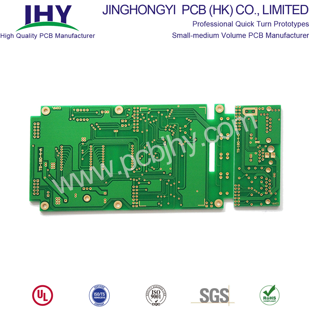
Generally, Thick Copper PCB means the finished copper thickness of the board is more than 4oz (140um), this is the most obvious factor to compare the thick copper board from standard PCB with 1oz or 2oz copper.
Heavy Copper PCB handles higher rates of current than other normal boards, are able to resist higher temperatures for longer time and provide stronger connection points.
JHY PCB is the well-known expert for Thick Copper Board, the maximum finished copper thickness can be 10 oz.
Please send email if request more detailed information of Extreme Copper PCB. Once tested the quality of our boards, you will know what we said is sincere.

Applications of Heavy copper-based PCB
- Solar arrays
- Power converters
- Power supplies
- Welding Machine
- Aviation
- Heavy machinery
- Automotive and more

Thick Copper PCB
Thick Copper PCB,Heavy Copper PCB,Copper Thickness PCB,Extreme Copper PCB
JingHongYi PCB (HK) Co., Limited , https://www.pcbjhy.com