The testing technology of integrated circuits has developed with the rapid development of integrated circuit development and application. Integrated circuit testers have also evolved from initial testing of small scale integrated circuits to testing of scale, large scale and very large scale integrated circuits. The integrated circuit tester can be divided into: digital integrated circuit tester, memory tester, analog and mixed signal circuit tester, online test system and verification system. At present, the tester products on the market have relatively simple functions and are very expensive, which brings inconvenience to the testing and maintenance of the circuit. Therefore, the research and development of simple and fast, intelligent IC tester has high practical value.
In the electronic experiment teaching of colleges and universities, medium-scale integrated circuits such as analog-to-digital converters (ADCs), digital-to-analog converters (DACs), 555 integrated timing circuits, and 3524 switching power supply controllers are often used. Since students usually use the chip for the first time, the circuit chip is often damaged or damaged due to improper operation, but the surface cannot be judged correctly. In this case, it is highly desirable to have a tester with an appropriate integrated circuit for testing and judging whether the chip is good or bad. There is no suitable tester available on the market. Therefore, this paper designed and manufactured a tester that can be used for some specific medium-scale circuits. According to the specific needs, ADC0809, DAC0832, LM555, WC3524 and other chips were selected as test objects, and corresponding special testers were designed.
The schematic block diagram of the tester is shown in Figure 1. The controller of the test instrument uses Atmel's eight-bit single-chip 89C55 for interface management and automatic detection and control functions [3]. Maxim's MAX197 high-precision A/D converter is used to complete the analog signal. Test [4]. The test principle and method of each type of device are introduced below.
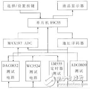
Figure 1 Test block structure block diagram
1 test principle and test circuit
To test the function or characteristic parameters of a device, usually take the typical application circuit of the device, reflect the function, and directly or indirectly reflect the parameter value.
1.1 Analog-to-Digital Converter ADC0809 Test
The test circuit diagram of the analog-to-digital converter ADC0809 is shown in Figure 2. According to the test circuit, the 8 channels of ADC0809 input the same analog quantity, and the analog quantity is also sent to the MAX197. The controller selects one analog channel of ADC0809, and sends a start conversion signal to start conversion of ADC0809, then control MAX197 also starts. Conversion. Wait for the end of the conversion, read the conversion results of the two, and compare the values ​​to determine whether the device function is normal according to the error limit. Change the channel to continue testing until the 8 channels are tested and the results are displayed.
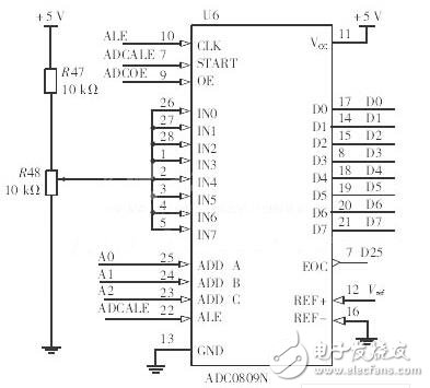
Figure 2 Test circuit diagram of ADC0809
1.2 DAC0832 test
The D/A converter DAC0832 is an 8-bit binary digital-to-analog converter. The eight digital inputs are DI7~DI0, of which DI7 is MSB and DI0 is LSB. Its analog output is current output IOUT1 and IOUT2. When the input digital maximum, the current output from IOUT1 is the largest; when the digital input is zero, the output current is the smallest. The current output at the IOUT2 ​​side is reversed. These two terminals can be connected to an external operational amplifier to achieve current/voltage conversion. There is also a feedback resistor inside the chip, which can be used as the feedback resistor of the external operational amplifier. The schematic diagram of the DAC0832 test is shown in Figure 3. There are two levels of input registers in the chip, which enable double buffering, single buffering and straight-through three input modes to suit various circuit needs, such as requiring multiple D/A asynchronous inputs, synchronous conversion, and the like.
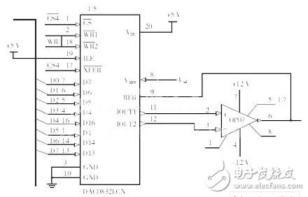
Figure 3 ADC0832 test circuit
When the 8-bit binary digital quantity is sent to the DAC0832 by the MCU, the D/A conversion is started when the write control and the chip select control of the two-stage buffer are both valid, and the conversion speed is microsecond. After the digital-to-analog conversion, the output current is converted into a voltage by the operational amplifier. The voltage is converted into a digital quantity by the MAX197 and read back into the single-chip microcomputer, and then compared with the digital quantity of the original output to determine whether the tested chip is normal or not.
1.3 LM555 timing circuit test
The integrated timing circuit LM555 is widely used, and its test circuit is shown in Figure 4. This is a typical timing circuit connection used to test whether the internal two comparators and RS flip-flops are normal and that the control voltage is normal.
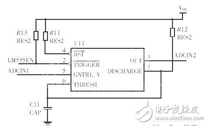
Figure 4 LM555 test circuit
The MCU outputs 1 negative pulse to the 2nd pin of the LM555 chip to trigger the timing circuit. The MCU reads the output signal of the timing circuit to determine whether there is a corresponding rising edge and falling edge, so that the function of the chip can be judged whether it is normal or not.
1.4 SG3524 test
The internal block diagram of the SG3524 is shown in Figure 5. The input DC power supply UIN enters from the 15th pin and is divided into 2 channels: one is used as the power supply for the amplifier, the comparator, the oscillator, and the logic circuit and the control circuit; the other is used as the reference voltage source, and the +5 V reference voltage is output to the 16-pin. As an external voltage reference. The timing capacitor CT and the timing resistor RT are externally connected to pins 7 and 6 of the oscillator section to obtain the desired oscillation frequency. The schematic diagram of the SG3524 test is shown in Figure 6. It is connected into a typical step-down switching power supply circuit, which uses the error amplifier to form a voltage negative feedback. The output voltage can be changed by changing the sampling proportional coefficient. The MCU can determine the quality of the SG3524 chip by measuring the pulse frequency on pin 3 and measuring the voltage at the output through the MAX197. The test of the overcurrent protection function was not considered in the test for the time being.
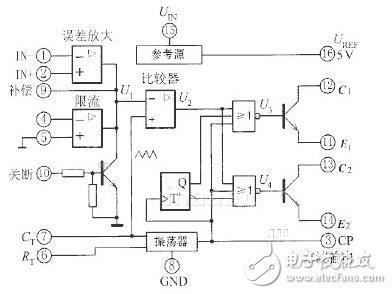
Figure 5 SG3524 internal block diagram
2 operation and software structure
The basic workflow of the tester is: after the power is turned on, the power indicator light is on, indicating that the power supply is working properly, and the display shows waiting for test information, indicating that the test operation can be started. The chip to be tested is selected by the button 1, and the chip model indicating the cursor staying is the current chip to be tested. Each time the selection button is pressed, the cursor points to the next model, and the button can be cycled continuously. When the cursor moves to the chip to be tested, press the OK button 2, and then the MCU controls to start the automatic test of the chip. At this time, the indicator light corresponding to the chip is bright; then the external circuit or the MCU gives a certain simulation to the chip to be tested. Or the digital input amount, after passing through the test circuit of each chip, is processed by the MAX197 (or directly sent to the single-chip microcomputer), and compared with the standard value pre-stored in the single-chip microcomputer. If the test value is within a certain range around the standard value, the chip is normal, the test indicator is always on, and the LCD display is OK; otherwise, the chip is faulty, the test indicator flashes, and the LCD display shows BAD. After the chip is tested, press reset. Key 3, returning to the initial state, can be tested in the next round. The software flow chart is shown in Figure 7.
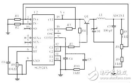
Figure 6 SG3524 test schematic

Figure 7 software flow chart
Features
A Push Button Switch is a switch that has a knob that you push to open or close the contacts. In some pushbutton switches, you push the switch once to open the contacts and then push again to close the contacts. In other words, each time you push the switch, the contacts alternate between opened and closed. These types are commonly called latching switches. There are also Non latching push button switches that only maintain the switch contacts when the switch is help in position. Once the switch is let go, the current is broken and the switch turns off. Push switches are usually a simple on-off switch.
Push On Off Switch,Small Push Button Switch,Automotive Push Switch,Miniature Push Button Switch
Ningbo Jialin Electronics Co.,Ltd , https://www.donghai-switch.com