Abstract: With the development of automobile industry and electronic technology, the degree of electronicization of vehicle-mounted systems is getting higher and higher. As an important part of human-computer interaction, car audio and video systems are becoming a new hotspot of research. This paper proposes an application scheme combining smart phone and car audio and video system, analyzes the hardware module and software flow chart of i.MX6 car audio and video system, and drives the initialization state machine. The system test results show that the audio and video system proposed in this paper realizes the basic functions of audio and video, and can also realize multi-screen interaction and provide real-time charging solution for mobile devices.
This article refers to the address: http://
In recent years, with the popularization of automobile users and the continuous innovation and development of electronic technology, people's performance requirements for automobiles have become higher and higher, from the traditional single function of vehicles to the multi-functional vehicles of multimedia and information; the automobile industry From simple mechanical products to optical and mechanical integration. The future trend is that the proportion of electronic products is continuously strengthened. As an important part of human-computer interaction, the car audio and video system has become a new hot spot of research.
At present, most of the car audio and video equipment on the market appears in the form of a complete audio and video system in the vehicle environment. This paper proposes a new scheme that uses Freescale Semiconductor's latest generation processor i.MX6 and combines the novel MHL protocol to study the car audio and video system, realizes multi-screen interactive function, and pays attention to prevent co-channel interference in multi-system applications. Problems and can provide real-time charging solutions for mobile devices.
1 i.MX6-based car audio and video system architecture
The system architecture based on the i.MX6 car audio and video system is shown in Figure 1. The car audio and video system designed in this paper consists of the original audio and video data source receiving module, data processing, video data and audio data output.
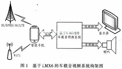
During normal operation, the system inputs audio and video data to the receiving module of the system through the integrated MHL-enabled smart phone. The data can be stored in the mobile phone's resources, or can be obtained from 2G, GPRS, 3G, LTE or WiFi networks. Audio and video data. The receiving module preprocesses the received data in the MHL format, separates the video data and the audio data in the data, converts the video data into a MIPI format, and converts the audio data into an I2S format.
The video data of the MIPI format and the audio data of the I2S format are simultaneously input into the processor i.MX6, and the video data is processed by the image processing subsystem, converted into RGB format video data recognized by the LVDS display, and output to the display through the LVDS cable. equipment. At the same time, an I2S receiving module of the processor receives the audio data, and the data is not processed, and is directly sent to the audio driver through another I2S sending module of the processor, and after being driven, the music synchronized with the video is played through the speaker or the earphone.
2 system hardware design
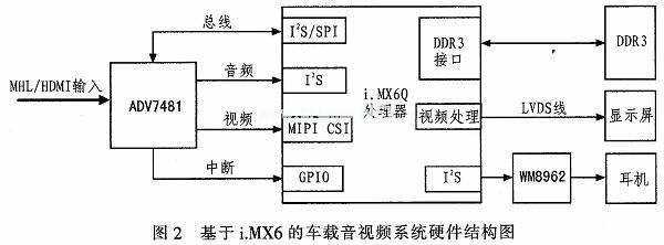
The system architecture based on the i.MX6 car audio and video system is shown in Figure 2. The hardware part of the car audio and video system based on i.MX6 mainly includes the MHL data format receiving module composed of ADV7481, i.MX6 processor module, display module, WM8962 audio driver module and power supply part.
2.1 Power section
The power supply part consists of two parts. The first part is the input overvoltage protection circuit to prevent the input voltage from being too large or external interference entering and damaging the circuit. The second part is the integrated voltage management circuit, which integrates the switching voltage conversion circuit and the linear voltage conversion circuit. .
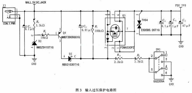
The input overvoltage protection circuit is shown in Figure 3. When the 5 V supply voltage is normally input, the switch S1 is closed, and the source of Q1 is 5 V. The gate voltage is determined by the voltage division of resistors R2, R4, and R5, which is about 0.26 V, so that the VGS of Q1 is -4.74 V, which is low. At the turn-on voltage of -2.1 V, the drain and source of Q1 are turned on, and the main power supply 5 V flows into the PSU_5V0 for later stage trial. When an abnormal overvoltage is input to the input terminal, the reverse voltage of the Zener diode D2 will exceed its reverse breakdown voltage limit, so that the cathode potential of D2 is stabilized at about 5.1 V, and the UBE of the transistor Q2 is greater than 0.7. At V, the collector and emitter of Q2 are turned on, and a large amount of current flows from inside. These currents will generate a voltage drop across R4 and R5, generating a voltage at the gate of Q1, making the gate of Q1 The source voltage is approximately equal, higher than the turn-on voltage of -2.1 V, and the Q1 tube is turned off, preventing overvoltage from flowing into the subsequent stage circuit, thereby realizing the function of protecting the latter stage circuit.
The integrated voltage management circuit selects Freescale Semiconductor's MMPF0100 solution, which mainly includes three parts: power management control, linear regulated power conversion, and switching power conversion. The management control part of the power supply can configure the output voltage value, accuracy, output timing, and the like. The essence of the switching power supply circuit is a series switching power supply. The linear regulated power conversion circuit is essentially a linear modulator.
2.2 Receiver module
The receiving module is compatible with both MHL and HDMI data source inputs. The differential data line of MHL and DATA0+/- of HDMI share a pair of differential lines. CBUS and HDMI_HPD_CON share one signal line, and the power and ground are shared.
The system determines the data source input by detecting the level of the CD_SENSE signal line on pin 2 of the connector. When CD_SENSE is high, it indicates that it is the MHL source input; when CD_SENSE is low, it indicates that it is the HDMI source input.
MHL has a special function, the Sink side can supply power to the Source device, and the 5 V voltage should be output to the outside. When the HDMI interface is compatible, it needs to receive the 5 V voltage of the Source device, which means that in two different input modes. The current direction of the 5V power pin is the opposite.
In order to solve the troubles caused by two different applications, this paper designs a 5 V power supply scheme, as shown in Figure 4. When the system detects the MHL input, CD_SENSE is high, Q7 is turned on, and the gates of Q7 and Q8 are about 0 V. Since Q7 has a body diode, the potential of Q7 and Q8 sources is only lower than 5 V. The turn-on voltage drop is still high, and the VGS of the two MOS transistors is greater than the turn-on voltage, and both are turned on. The 5 V power supply charges the Source device through the power pin of the connector. When the system detects the HDMI input, CD_SENSE is low, Q6 tube is off, there is no current on R15, Q3 and Q4 source and gate voltage are equal, all are off state, 5 V can not supply power, power pin only Receive the voltage of the Source to implement the detection function.

2.3 i.MX6 processor module
This article uses Freescale's i.MX6 processor, which integrates a 4-core ARM Cortex-A9 with advanced nanotechnology and a maximum speed of 1.2 GHz per core. Each processor provides a 64-bit memory interface and a range of peripheral interfaces. Such as MIPI CSI-2 interface, I2S interface, wireless interface, display interface, camera sensor interface, etc. It can be seen from the characteristics of this chip that it has high speed, security, low power consumption, integrated multiple peripheral interfaces on the chip, and rich resources, which can meet the growing in-vehicle entertainment, remote information access and processing, human-computer interaction interface, The market demand shown by the cluster.
Guard bar
Guard bar
Jiangsu Bosiwei Optoelectronics Group Co.,ltd , https://www.bswledled.com