First, the design of the tube preamplifier
This article refers to the address: http://
The electron tube is an amplifying device with high input impedance, high operating voltage and easy aging. It is more difficult to design a tube preamplifier that can meet the Hi-Fi standard than the crystal preamplifier.
Pay special attention to the following points when designing:
1. Reasonable selection of electronic tubes: There are many types and models of electronic tubes. Each type of tube has different performance, structure, working conditions and use occasions, and has certain timbre differences. Because of this, different tubes cannot be used interchangeably. In the preamplifier, the triode should generally be used, because the triode has good linearity, low noise, and the amplification factor is not too high. It can be used for audio amplification to obtain better comprehensive performance and sound quality, and the circuit is relatively simple. There are many types of triodes. Which one is selected depends on the circuit structure and gain. The gain of a triode amplifier is generally about 0.6 μ, and its μ value is mostly between 20 and 100, so the amplification factor generally does not exceed 70. If the circuit only needs to be amplified one step, a triode with a higher μ value can be selected, and a multi-stage amplifier can be selected. It is better to use medium μ or low μ tube to obtain better stability. Some European and American brands of old-fashioned electronic tubes have been heated up by the media, and the prices have been doubling. It seems that only the pipes of these brands are the most popular. In fact, there are many factors for artificial speculation.
China has decades of experience in the production of electronic tubes. It is the world's largest producer of electronic tubes. The life of pipes has reached 10,000 or even more than 100,000 hours. Many brands are also regarded as treasures by foreign enthusiasts. Therefore, in the selection, this problem should be viewed scientifically and sensibly, to avoid people's clouds and clouds, and to listen to partial beliefs. As far as the triode is concerned, the domestically produced 6N1, 6N2, 6N3, 6N4, 6N6, 6N11, etc. are very good performance tubes, and as long as the application is reasonable, the same sound quality can be obtained. What's more, the performance of many foreign second-hand pipes that are popular on the Internet is almost at the end of life.
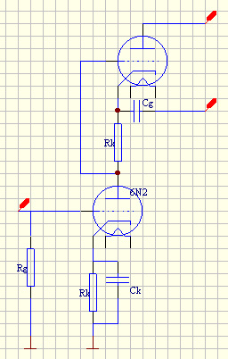
This production tube is locked in 6N2, 6N2 is a very good audio amplifier tube, it is basically the same as the 12AX7 parameters, the sound is similar, only the filament pin is different, it is also very simple to replace the 12AX7 in use. 6N2-PDF file
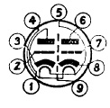
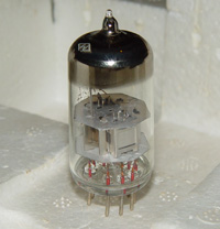

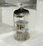
6N2 pin 6N2 appearance (Shanghai) 6N2 appearance (Dawn) 6N2 appearance (Beijing)
2. Proper selection of operating points: As with transistors, the operating point of the tube amplifier should also be chosen to have the lowest distortion and large dynamic range. Since each tube has different characteristic curves, it has its own optimal working point. The selection should be carried out according to the characteristic curve given in the manual and the established method to ensure that the tube can work optimally within the dynamic range. But the audio equipment is used to restore music, loyal to the original is its vocation, the technical specification of the finished product is the designer's second criterion, but its manufacture is different from the general electrical design, and it needs to be based on the technical specifications. The "artistic spirituality" of the product.
The voltage amplification of the tube, when there is a slight change in the gate voltage, the screen will have a large variation. In other words, the influence of the gate voltage on the screen current is very large, and there is no audio signal input in the gate circuit. When the screen current is stable DC, and the gate voltage is negative, the screen current is smaller. When the gate voltage is negative to a certain extent, the screen current will be equal to zero in the off state. If the audio signal U is input in the gate circuit, the gate is The potential between the pole and the cathode will change constantly, and the screen current will also change. On the R1 of the screen circuit, in addition to the DC voltage drop of its own working power supply, an audio AC voltage drop is added. The value of Rl is selected to obtain the amplified signal voltage.
In actual production, it is found that the actual characteristics of domestically produced 6N2 with different brands are very different (more details below), and on the other hand, the quality difference of individual domestic brand devices is also reflected.
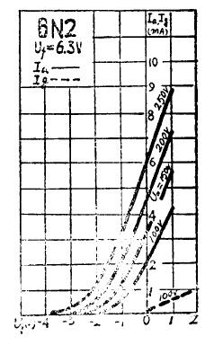
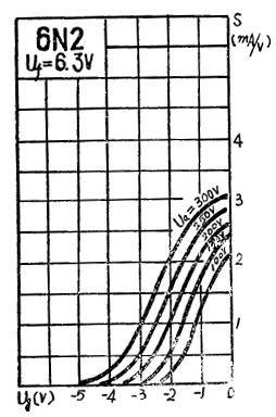

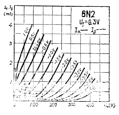
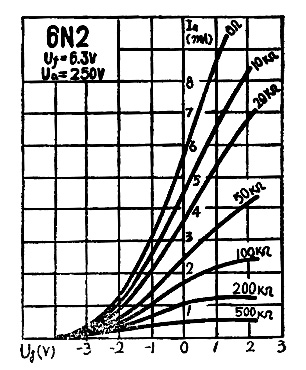
Characteristic curve (0) characteristic curve (1) characteristic curve (2) characteristic curve (3) characteristic curve (4)
3. Adopt effective noise reduction measures: the input impedance of the tube is very high, and the cathode must be heated, which is easy to sense or introduce various AC interference noise, so the signal-to-noise ratio (S/N) of the tube amplifier is difficult to do well. This is especially true for preamplifiers.
At present, the most effective noise reduction measures are:
(1) Power the filament with a regulated power supply. The bypass heating tube generally uses an AC power source to supply power to the filament. Thus, due to the existence of parasitic capacitance between the filament and the gate, the alternating current charges and discharges the capacitor, which causes a voltage drop across the gate resistor, resulting in a large hum. In addition, the filament emits a small amount of electrons (especially at both ends of the filament) at normal operating temperatures. These electrons fly to the inner wall of the cathode sleeve, and then enter the ground through the cathode resistor to form AC interference. If the cathode capacitance is not large or there is no cathode capacitance, the AC interference is not effectively suppressed. If a DC stabilized power supply is used, if a regulated power supply composed of a three-terminal voltage regulator is used to supply the filament, it is possible to avoid the hum caused by the above reasons, so that the S/N is significantly improved.
(2) Lower the potential between the filament and the gate. If you do not want to use DC voltage regulation to supply the filament, you can use a conventional method to connect a (50~100) Ω wirewound potentiometer to both ends of the filament power supply, and ground the sliding arm to reduce the potential between the filament and the cathode. To reduce the impact of AC power on S/N. In addition, grounding one of the filament pins of the input stage tube can also achieve a similar effect.
(3) The purpose of adding a certain positive voltage and a positive voltage to the center tap of the filament winding is to make the filament have a positive potential to the cathode, and pull the electrons emitted by the filament back to the filament to suppress the hum generated by the filament emitting electrons. In addition, it is also effective to appropriately reduce the supply voltage of the filament within the allowable value.
(4) Improve the filtering effect of the screen power supply. Nowadays, high-voltage, large-capacity electrolytic capacitors are at your fingertips, and the capacity of the screen power supply filter capacitor can be used to a larger extent, such as 220 μF or more. If it is a multi-stage amplifier, the method of sub-level decoupling filtering can be used to improve the filtering effect of the screen power supply. Choke coil filtering can also be used for higher requirements until it is powered by a regulated power supply.
(5) Reduce the interference of stray electromagnetic fields on the circuit. Electromagnetic field interference is also a major factor affecting S/N. Therefore, high-quality preamplifiers should use power transformers with low electromagnetic interference. The gate signal leads should be as short as possible and shielded wires should be used. It is best to add a shield to the input stage tube. The filament leads are twisted and away from the grid.
(6) Avoid interference with the ground loop that is not properly grounded. The effects of various AC interferences entering the gate loop through the ground loop on S/N may be greater than other factors and should be highly valued. For a simpler amplifier, the most effective way to avoid ground interference is to use a little grounding, that is, the input signal is soldered to the ground point of the gate, cathode, and cathode capacitors, and then with the power filter capacitor. Connect the grounding point to the chassis. For multi-stage amplifiers, the grounding points of each level can be collected at one point, and then the grounding points of the stages are connected to the power ground in the order from the front stage to the rear stage, and then connected to the casing. The best point to connect to the chassis may be the power ground or the input ground. Which one is better is generally determined experimentally.
4. Ensure that the resistor block has sufficient power dissipation or withstand voltage
Although the working current of the preamplifier tube is only a few milliamperes, the screen power supply voltage is generally above 200V, and the power consumption is still considerable. Therefore, it should be ensured that the power dissipation of the resistor used in the circuit and the withstand voltage of the capacitor are sufficiently large. When selected, the value of both should generally be more than twice the actual power consumption and the applied voltage. Otherwise, the reliability will decrease.
Analysis and calculation of the second and triode preamplifier circuit
The triode voltage amplifying circuit is usually composed of a one-stage or multi-stage resistance-capacitance coupling voltage amplifying circuit and an impedance converting circuit, and some also have a negative feedback circuit. By mastering the principles and calculation methods of these basic circuits, various preamplifiers can be designed according to actual needs.
Commonly used voltage amplifying circuits are a common cathode amplifying circuit and an SRPP amplifying circuit. The following is a brief introduction of the working principle and calculation method.
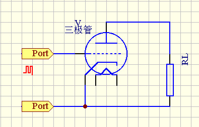
A) RC-coupled common cathode amplifier circuit
The common cathode amplifying circuit can be composed of a triode or a pentode, but the common cathode circuit composed of the five-stage tube is generally only used for the post-stage amplifier due to the large noise.
1 Working principle
When a signal voltage is applied to the gate of the valve, the current flowing through the screen circuit is generated. When ia flows through Ra, a voltage drop Ua is generated on Ra, which is the amplified signal voltage. The phase change of its amplitude is opposite to ia. When the screen voltage changes from high to low, the capacitor Ca discharges; when the screen voltage changes from low to high, the capacitor Ca is charged. The voltage drop U generated on the RL when the charge and discharge currents are injected through the RL. This is the output signal voltage of the circuit. If the amplifier is composed of a two-stage common cathode circuit, RL is the gate voltage Rg of the second-stage electron tube, and the signal voltage U is output. The second stage valve grid will be added for further amplification.
2 Calculation method
As a high-fidelity tube amplifier, we want its frequency response to be as wide as possible. The low-frequency response of the electron tube is mainly determined by the input coupling capacitor Cg, the output coupling capacitor Ca and the cathode bypass capacitor Ck. The values ​​of Cg and Ca should meet the following requirements, namely:
Cg(Ca)≥1/2πfLRg
In the formula, the lower limit frequency of the fL amplifier is generally 20 Hz, and Rg is the value of the gate bias resistance. When calculating Ca, Rg is the value of the gate bias resistance of the subsequent stage of the tube. The cathode resistance Ck can be estimated by the following formula:
Ck≥(3~5)/2πfLRk
The high frequency response is mainly caused by the load resistance R'a. And the distribution capacitance Co is determined. Its high-end cutoff frequency is:
fH = 1/2Ï€R'aCo
It can be seen that the smaller Co or R'a, the wider the frequency response. The value of Co varies depending on the form of the tube and the circuit used. It is approximately equal to the sum of the output capacitance of the screen and the input capacitance of the next stage. Therefore, an electron tube with a small input and output capacitance should be selected, and the distributed capacitance formed by the wiring should be minimized. R'a is more favorable for high-frequency response, but it should not be too small, because the voltage amplification factor of the tube is KO=SR'a. When R'a is small, KO is numerically equal to the internal resistance Ri, Ra and The parallel value of the primary gate resistor, ie:
1/ Ugm2=1/Ra+1/Ri+1/R'a
The value of Ra can be selected between (50~500) KΩ, and the maximum allowable value of R'a is generally:
R'a=Ri·τa/(CoRi—τa)
Where Ï„a is the time constant of the tube screen and its value is:
Τa =
In the formula, M is the frequency distortion coefficient, which is generally taken from 1.1 to 1.26.
The gate bias of the electron tube can be obtained by the following equation, namely:
Eg≥1+Ugm2/0.7μ
Where, Ugm2 is the maximum input voltage required for the lower stage or the output voltage of the current stage, and μ is the amplification factor given in the manual. The absolute value of the gate negative voltage should generally be larger than the input signal voltage amplitude (0.5~1)V, so as to prevent the electrons emitted from the cathode from hitting the gate and a gate current.
In general, the gate resistance of the next stage and the AC screen voltage of the local pole can be taken separately:
R'a = (5~10) Ra
Ua = (0.33~0.5) Ea
After the grid negative pressure is determined, a static and dynamic load line can be made on the screen characteristic curve of the tube, and Ri, S, and μ decibel values ​​are obtained at the working point. If Ri differs greatly from the above set values, R'a should be recalculated.
At this time, the voltage amplification factor Kz of the intermediate frequency region can be calculated by the following equation.
Kz=μ/(1+Ri/Rg+Ri/Ra)
Then, the value of the cathode self-bias resistor is obtained according to the operating point current Io and the gate negative voltage, that is,
Rk=Ez/Io
Due to the nonlinearity of the tube characteristic curve, the output current waveform that is not proportional to Ia and Ug is generated, resulting in nonlinear distortion. At this time, it is more convenient to analyze the nonlinear distortion by using the line segment of the dynamic characteristic curve instead of the ordinate indicating the current. Therefore, these current values ​​can be represented by corresponding line segments, and the degree of asymmetry of the line segments reflects nonlinear distortion. the size of.
B) SRPP voltage amplifying circuit
1) The special circuit structure of the circuit was originally designed for high-frequency amplifiers. Because of its low distortion, low noise, wide frequency response, etc., it can adapt to high fidelity requirements, so it is used by many modern tube audio amplifiers.
The DC paths of the upper and lower tubes are connected in series. The lower tube constitutes a triode common cathode voltage amplifying circuit, and the upper tube constitutes a cathode output circuit and serves as a constant current load of the lower tube. Its input signal is provided by the screen of the lower tube and then by the cathode of the upper tube. Since the voltage amplification factor of the cathode follower is close to 1, the voltage amplification factor of this circuit depends on the lower tube, which is similar to the general triode amplification circuit, but its output has a low cathode resistance, greatly improved load capacity, and easy and low resistance load. match. Since the voltages of the upper and lower tubes are simultaneously output from the cathode of the upper tube, this circuit is also called a parallel adjustment push-pull circuit. Its special structure reduces the influence of the distributed capacitance of the tube on the high frequency. The high frequency response can be more than three times the width of the general triode circuit. However, since the cathode voltage of the upper tube is about 1/2 Ea, it has exceeded the cathode and filament of the general tube. The voltage limit value, so it is best to let the lamp ribbon suspend the positive potential of about 70V when applied. Otherwise, the reliability is poor.
2) Calculation method
Since there is no negative feedback, Ri=△Ua/△Ia; when there is negative feedback, the screen current is ΔIa/(1+S RK). Therefore, the internal resistance of the upper tube
Ri=△Ua/[△Ia/(1+S RK)]= Ra+μRK
This Ri is the load of the lower tube, which is equivalently connected in parallel to the screen of the lower tube during AC, so the voltage amplification factor
KV=SRa(Ra+μRK)/(Ra+ Ra+μRK)
=μ(Ra+μRK)/(2Ra+μRK)
Considering the load access, the magnification will be reduced.
KV=μ(Ra+μRK)/(Ra+RK)(Ra+RL+1)(Ra+μRK)
The output impedance of the circuit, etc., is equal to the ratio of the amount of change ΔUo of the output voltage to the sum of the total current change amount ΔI1 of the upper and lower tubes and the current change amount ΔI2 generated by the lower tube. which is:
Ro=â–³Uo/(â–³I1+â–³I2)
After a series of deductions, you can get:
Ro=Ra(Ra+RK)/[2Ra+(1+μ)RK]
The calculation of other parameters can be carried out by referring to the calculation method of the triode voltage amplifying circuit.
Flash Gold+Hard Gold board. the base Material is FR4 IT180A (TG180). 8-layer PCB.Copper thickness is 1oz inner-layer/1.5oz outer-layer.Board Thickness is 1.8mm and the Min.Hole Size is 0.3mm. Min.Line Width/Min.Line Spacing is 0.25mm/0.25mm. green solder-resist & white silkscreen. E-test: 100%. Flash Gold(hard Gold) is an expensive surface treatment, which has the advantage of being able to withstand friction.
")
Flash Gold(hard Gold)
Flash Gold,Custom Flash Gold,Hard Gold,Stick Flash Gold
Orilind Limited Company , https://www.orilind.com